


 Trouble in Your Tank: Understanding Interconnect Defects, Part 1
 It’s Only Common Sense: Marketing Isn’t Fluff, It’s Ammunition
 Driving Innovation: Mechanical and Optical Processes During Rigid-flex Production


Pioneer Circuits’ Solutions Used in NASA's PUFFER Collapsible Bot
February 5, 2018 | Pioneer CircuitsEstimated reading time: 2 minutes
The PUFFER (Pop-Up Flat Folding Explorer Robot) collapsible micro-rover is a part of NASA’s “Game Changing Development Program.” It is a compact rover that will ride on board with future space vehicles to land on space bodies such as planets and asteroids for photographs and microanalysis.
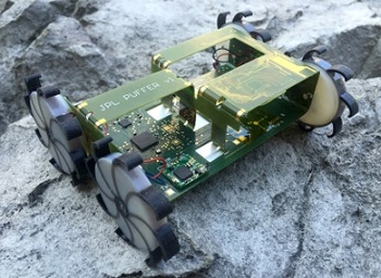
Figure 1: The original PUFFER prototype before working with Pioneer Circuits for the new hinge technology.
The PUFFER micro-rover utilizes a new, patented hinge technology containing a high-temperature woven fabric that is compatible with PWB rigid-flex manufacturing. JPL utilized Pioneer Circuits’ concurrent engineering services to help with the new developments that were a key enabler for the PUFFER project.
The Challenge
The PUFFER’s concept addresses the challenge of developing robotic mobility in space exploration. The PUFFER challenge was to design a micro-rover capable of surviving the harsh environments of deep space while also being able to collapse and fold into more compact forms that will fit into small areas for detailed photographs and surface analysis.
The original PUFFER prototypes were having issues with passing their cycle and drop test operations. Design challenges included the mechanical design of the rigid-flex PCB joints to be able to work on a repeatedly folding robot structure, and for the PCB’s copper traces to last the lifetime of the rover. The original materials used for the joints were not compatible with current PCB manufacturing processes, and the PUFFER was only able to withstand 1,000 test cycles—a very conservative number for a Mars application.
Through concurrent engineering, Pioneer Circuits found the material and developed a high-temperature woven fabric hinge technology that is compatible with PCB rigid-flex manufacturing. The rigid-flex circuit technology is integrated into a highly reliable, composite structure that is the first origami micro-rover configuration ever developed.
Figure 2: A close-up of Pioneer Circuits and JPL’S hinge technology with woven fabric.
To make the technology possible, Pioneer Circuits developed new bonding and process capabilities that are compatible with this unique challenge. Integration of the high-temperature woven material as a layer in the PCB stack-up allowed the mechanical and electrical functions to overcome limitations of typical polyimide builds. Using the material as a hinge would makes the PUFFER more reliable and able to repeatedly collapse without damaging the copper traces. The new PUFFER design was capable of withstanding drop-testing that simulated the harsh space body environments, and was is able withstand over 5,000 cycle tests—500% more than the original designs.
Figure 3: The final full and collapsed version of the PUFFER microrover.
Impact
Pioneer Circuits’ work with JPL on the development of the PUFFER has resulted in technology that is now being patented. The PUFFER micro-rover will now be able to ride on board with future space missions for thorough surface analysis. The collapsing capability allows the PUFFER’s microcamera to focus for microanalysis. This “Game Changing” development will give NASA and JPL a less-expensive opportunity to explore the surfaces of space that were never before reached.
Share on:


Testimonial
"Your magazines are a great platform for people to exchange knowledge. Thank you for the work that you do."
Simon Khesin - Schmoll MaschinenSuggested Items
Trouble in Your Tank: Understanding Interconnect Defects, Part 1
11/04/2025 | Michael Carano -- Column: Trouble in Your TankThis month, I’ll address interconnect defects (ICDs). While this defect continues to rear its ugly head, don’t despair. There are solutions, most of which center on process control and understanding the relationship of the chemistry, materials, and equipment. First, though, let’s discuss ICDs.
WestDev Announces Advanced Thermal Analysis Integration for Pulsonix PCB Design Suite
10/29/2025 | WestDev Ltd.Pulsonix, the industry-leading PCB design software from WestDev Ltd., announced a major enhancement to its design ecosystem: a direct interface between Pulsonix and ADAM Research's TRM (Thermal Risk Management) analysis software.
Designers Notebook: Power and Ground Distribution Basics
10/29/2025 | Vern Solberg -- Column: Designer's NotebookThe principal objectives to be established during the planning stage are to define the interrelationship between all component elements and confirm that there is sufficient surface area for placement, the space needed to ensure efficient circuit interconnect, and to accommodate adequate power and ground distribution.
Episode 6 of Ultra HDI Podcast Series Explores Copper-filled Microvias in Advanced PCB Design and Fabrication
10/15/2025 | I-Connect007I-Connect007 has released Episode 6 of its acclaimed On the Line with... American Standard Circuits: Ultra High Density Interconnect (UHDI) podcast series. In this episode, “Copper Filling of Vias,” host Nolan Johnson once again welcomes John Johnson, Director of Quality and Advanced Technology at American Standard Circuits, for a deep dive into the pros and cons of copper plating microvias—from both the fabricator’s and designer’s perspectives.
Nolan’s Notes: Tariffs, Technologies, and Optimization
10/01/2025 | Nolan Johnson -- Column: Nolan's NotesLast month, SMT007 Magazine spotlighted India, and boy, did we pick a good time to do so. Tariff and trade news involving India was breaking like a storm surge. The U.S. tariffs shifted India from one of the most favorable trade agreements to the least favorable. Electronics continue to be exempt for the time being, but lest you think that we’re free and clear because we manufacture electronics, steel and aluminum are specifically called out at the 50% tariff levels.