


 It’s Only Common Sense: If You’re Not Differentiated, You’re Dead
 Alpha Insights, Performance by Design: The Future of PCB Manufacturing in the Midwest
 Happy’s Tech Talk #43: Engineering Statistics Training With Free Software


Building Miniature Optical Antennas Using DNA as a Guide
February 5, 2018 | University of JyväskyläEstimated reading time: 2 minutes
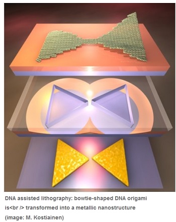
A new fabrication technique combines programmable DNA origami shapes and conventional lithography methods to create metallic nanoantennas and chiral shapes for diverse applications.
Research groups from University of Jyväskylä and Aalto University (Finland) together with researchers from California Institute of Technology (Caltech, USA) and Aarhus University (iNANO Center, Denmark) have reported a new highly parallel technique to fabricate precise metallic nanostructures with designed plasmonic properties by means of different self-assembled DNA origami shapes. The so-called DALI (DNA-assisted lithography) method has been published in the latest issue of Science Advances.
“We can build virtually any nanoscale shape using a DNA origami technique, and now we have shown how to use these accurate shapes as “stencils” to create millions of fully metallic nanostructures with 10 nm feature sizes in one go”, explains Adjunct Professor Veikko Linko from Aalto University. The trick in the DALI method is that when the DNA structures are deposited on a chip coated with silicon, silicon oxide can be selectively grown only on the bare areas of the substrate. “By controlling this process, we can create origami-shaped openings on the grown silicon oxide layer, and this layer can be used as a mask for the following lithography steps. Finally, we evaporate metal through these openings and create metallic structures having the same shape and size as the original DNA origami on a transparent substrate, such as sapphire”, Boxuan Shen from the Nanoscience Center of University of Jyväskylä describes the method.
The tiny metallic features cover the whole transparent substrate, and therefore these surfaces have intriguing optical properties. The small dimensions of the structures – in the range of ten nanometers – allow further tuning of these properties at the visible wavelength range. “Actually, we have demonstrated here a structure that we believe is the world’s smallest entirely metallic bowtie-shaped antenna. This extremely small size extends the operating range of optical features from infrared to visible”, states Adjunct Professor Jussi Toppari from Molecular Electronics and Plasmonics group at University of Jyväskylä. These antennas can find use in dozens of optical and plasmonic applications, such as surface enhanced Raman spectroscopy, biosensing or fluorescence enhancement. Moreover, the researchers demonstrated that the surfaces can be used as polarizers by fabricating chiral structures using DALI.
“The DALI method is highly parallel, and it could further enable cheap wafer-scale production of surfaces as it does not rely on costly patterning methods. It is also equipped for the future studies to provide bioinspired surfaces and metamaterials if the customized origami structures can be arranged on the substrate before metallization”, envisions Professor Mauri Kostiainen from the Biohybrid Materials Group at Aalto University.
Share on:


Testimonial
"In a year when every marketing dollar mattered, I chose to keep I-Connect007 in our 2025 plan. Their commitment to high-quality, insightful content aligns with Koh Young’s values and helps readers navigate a changing industry. "
Brent Fischthal - Koh YoungSuggested Items
Is Glass Finally Coming of Age?
10/13/2025 | Nolan Johnson, I-Connect007Substrates, by definition, form the base of all electronic devices. Whether discussing silicon wafers for semiconductors, glass-and-epoxy materials in printed circuits, or the base of choice for interposers, all these materials function as substrates. While other substrates have come and gone, silicon and FR-4 have remained the de facto standards for the industry.
Interposers, Substrates, and Advanced Manufacturing
10/13/2025 | Marcy LaRont, I-Connect007I attend a lot of industry trade shows and conferences. Lately, during conversations with technologists, I’ve noticed that there is some confusion about what exactly constitutes an interposer. One question I hear every so often is, “Are all interposers substrates?” The short answer to that question is no. But some interposers are, in fact, full substrates.
SCHMID Advances Next-Gen Advanced Packaging with New InfinityLine and Glass Core Substrate Solutions
09/29/2025 | SCHMID GroupSCHMID Group, a leading global provider of equipment and solutions for the electronics industry, announces a major expansion of its product portfolio to meet the surging demand for two types of products: Advanced packaging substrates and high-performance server boards, in the era of Artificial Intelligence (AI).
New Podcast Episode Drop: MKS’ Atotech’s Role in Optimize the Interconnect
09/08/2025 | I-Connect007In this episode of On the Line With…, host Nolan Johnson sits down with Patrick Brooks, MKS' Atotech's Global Product Director, EL Systems, to discuss the critical role that wet processes play alongside laser systems in advancing the Optimize the InterconnectSM initiative. Brooks points to Bondfilm as a key example—a specialized coating that enables CO₂ lasers to ablate more effectively than ever before.
New Episode Drop: MKS’ ESI’s Role in Optimize the Interconnect
08/26/2025 | I-Connect007In this latest episode, Casey Kruger, director of product marketing at MKS’ ESI, joins On the Line With… host Nolan Johnson to share how CO₂ laser technology delivers faster, more accurate vias in a smaller, more energy-efficient footprint.