


 The Right Approach: I Hear the Train A Comin'
 It’s Only Common Sense: OCCAM—the Time Is Now
 Marcy's Musings: The Growing Industry
Leveraging Imperfections to Create Better-Behaved Quantum Dots
May 23, 2018 | University of Wisconsin-MadisonEstimated reading time: 2 minutes
Potentially paving the way toward advanced computers, lasers or optical devices, University of Wisconsin-Madison researchers have revealed new effects in tiny electronic devices called quantum dots.
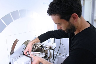
Image caption: Postdoctoral scholar Anastasios Pateras adjust an X-Ray instrument used to detect previously unknown defects in quantum dots. Photo credit: Sam Million-Weaver.
The researchers developed and applied analysis methods that will help answer other challenging questions for developing electronic materials.
“We can now look at a set of structures that people couldn’t look at before,” says Paul Evans, professor of materials science and engineering at UW-Madison. “In these structures, there are new sets of crucial materials problems that we previously weren’t able to think about solving.”
The structures Evans and colleagues looked at are thousands of times narrower than single sheets of paper, and smaller than the dimensions of individual human cells. In those structures, quantum dots form inside very thin stacks of crystalline materials topped by an asymmetrical arrangement of flat, spindly, fingerlike metallic electrodes. Between the tips of those metallic fingers are small spaces that contain quantum dots.
Creating such precise structures and peering inside those tiny spaces is technically challenging, however, and quantum dots don’t always behave as expected.
Previous work by Evans’ collaborators at the Delft University of Technology in the Netherlands, who created and extensively studied the crystal stack structures, led to suspicions that the quantum dots were different in important ways from what had been designed.
Until now, measuring those differences wasn’t possible.“Previous imaging approaches and the modeling weren’t allowing people to structurally characterize quantum dot devices at this tiny scale,” says Anastasios Pateras, a postdoctoral scholar in Evans’ group and the paper’s first author.
Pateras and colleagues pioneered a strategy for using beams of very tightly focused X-rays to characterize the quantum dot devices—and that hinged on a new method for interpreting how the X-rays scattered. Using their approach, they observed shifts in the spacing and orientation of atomic layers within the quantum dots.
“Quantum dots need to be close to perfect,” says Evans. “This small deviation from perfection is important.”
The team’s discovery indicates that the process of creating the quantum dots—laying down metallic electrodes atop a lab-grown crystal—distorts the material underneath slightly. This puckering creates strain in the material, leading to small distortions in the quantum dots. Understanding and exploiting this effect could help researchers create better-behaved quantum dots.
“Once you know these quantities, then you can design devices that take into account that structure,” says Evans.
Designs with those small imperfections in mind will be especially important for future devices where many thousands of quantum dots must all work together.
“This is going to be very relevant because, right now, there are multiple sources of decoherence quantum dots,” says Pateras.
The researchers now are developing an algorithm to automatically visualize atomic positions in crystals from X-ray scattering patterns, given that performing the necessary calculations by hand would likely be too time-consuming. Additionally, they are exploring how the techniques could add insight to other hard-to study structures.
Share on:


Suggested Items
Inkjet Solder Mask ‘Has Arrived’
04/10/2024 | Pete Starkey, I-Connect007I was delighted to be invited to attend an interactive webinar entitled “Solder Mask Coating Made Easy with Additive Manufacturing,” hosted by SUSS MicroTec Netherlands in Eindhoven. The webinar was introduced and moderated by André Bodegom, managing director at Adeon Technologies, and the speakers were Mariana Van Dam, senior product manager PCB imaging solutions at AGFA in Belgium; Ashley Steers, sales manager at Electra Polymers in the UK; and Dr. Luca Gautero, product manager at SUSS MicroTec Netherlands.
NetVia Group Acquires Direct Imaging from Mivatek
04/09/2024 | Miva TechnologiesMiva Technologies is pleased to announce NetVia Group, Irving, TX has acquired a new Miva 2400NG Dual Tray Direct Imaging System with 30-micron capabilities for inner, outer and soldermask imaging.
Teledyne to Acquire Adimec
02/13/2024 | TeledyneTeledyne Technologies Incorporated announced that it has entered into an agreement to acquire Adimec Holding B.V. and its subsidiaries.
Real Time with... productronica 2023: MivaTek Global Advances Technology With High-res Imaging System
12/08/2023 | Real Time with...productronicaMivaTek's Brendan Hogan talks about how the company employs Digitally Adaptive Rasterization Technology (DART) in their high-res imaging equipment. He also shares how the blurred line between semiconductors and microelectronics is driving broader application of the imaging process.
Keysight Enables Validation of Arbe 4D Imaging Radar Chipset
11/30/2023 | Keysight Technologies, Inc.Keysight Technologies, Inc. announces that Arbe has selected the E8719A Radar Target Solution (RTS) to test the Arbe 4D imaging radar chipset for automotive applications.