


 Dan’s Biz Bookshelf: ‘The Next RenAIssance: AI and the Expansion of Human Potential’
 The Chemical Connection: When the Industry Moves Faster Than the Standards
 Driving Innovation: Selecting the Right Laser Source


Atotech to Introduce Cupracid Flex and InPro Flex
June 13, 2018 | AtotechEstimated reading time: 2 minutes
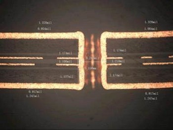
The flex/ flex-rigid PCB market continues to grow as more and more designs call for flexible inner layers with ever finer lines and spaces. At the same time, the need for high volume reel to reel formats as well as pattern plating with lower base copper thickness drives the FPCB market.
As one of the market leaders for BMV filling and through hole filling in the IC-substrate market, Atotech has developed two new acid copper processes – InPro Flex and Cupracid Flex – to serve the flexible printed circuit board market and support its customers to overcome the current technical barriers in FPCB manufacturing.
Excellent throwing power: Board thickness: 0.3mm, Hole: 0.15mm, CD: 2.8ASD, Line speed: 0.6m/min, Flow rate: 15HZ, Average TP% : 120%
Cupracid Flex and InPro Flex
“Cupracid Flex and InPro Flex are specifically designed for standard conformal flex and rigid-flex applications. While the Cupracid Flex process is for use in vertical systems with soluble anodes, InPro® Flex can be used in systems with insoluble anodes,” states Mustafa Oezkoek, Global Product Manager Panel and Pattern Plating at Atotech Deutschland GmbH.
The simple two additive processes can be analyzed by standard CVS method and are suitable for vertical equipment or vertical reel to reel equipment with educator or sparger systems. They can be operated in panel and pattern plating and provide excellent line shape, outstanding crystal structure and a ductility of more than 23% in either manufacturing method.
Features and Benefits
“Cupracid Flex and InPro Flex are highly reliable processes and deliver excellent physical properties,” continues Mustafa. “Both solutions assure first-rate throwing power at high current densities without any corner flattening. At the same time, pattern uniformity and line shape are very good. And, according to IPC, the bending performance is exceptional.”
Both products have been rolled out globally and are available worldwide.
About Atotech
Atotech is one of the world’s leading manufacturers of specialty chemicals and equipment for the printed circuit board, IC-substrate and semiconductor industries, as well as for the decorative and functional surface finishing industries. Atotech has annual sales of USD1.2 billion (2017). The company is fully committed to sustainability – we develop technologies to minimize waste and to reduce environmental impact. Atotech has its headquarters in Berlin, Germany, and employs about 4,000 people in over 40 countries. About a quarter of all staff works in one of the four locations in Germany: Berlin, Feucht, Neuruppin, and Trebur. For more information, click here.
Share on:


Testimonial
"The I-Connect007 team is outstanding—kind, responsive, and a true marketing partner. Their design team created fresh, eye-catching ads, and their editorial support polished our content to let our brand shine. Thank you all! "
Sweeney Ng - CEE PCBSuggested Items
Driving Innovation: Selecting the Right Laser Source
04/28/2026 | Simon Khesin -- Column: Driving InnovationWhen I first joined Schmoll Maschinen, I brought experience from almost every PCB process, except for laser. As I immersed myself in laser processing, I realized why it can seem so daunting to a newcomer. The complexity arises from three intersecting factors: A vast variety of laser sources: CO2, UV-nano, green-pico, UV-pico, IR-pico, and others; a diverse range of applications: Drilling, cutting, ablation, and more; and an extensive list of materials: These have vastly different absorption rates. Choosing the right machine or laser source is rarely trivial. Even for experienced engineers, answering "Which source is best?" requires examining the business's specific goals.
Institute of Circuit Technology Spring Seminar 2026: A Bright Future in Europe
04/23/2026 | Pete Starkey, I-Connect007Through the leafy lanes and spring flowers of Warwickshire and back to Meridan, the traditional centre of England, and now officially part of the Metropolitan Borough of Solihull in the county of the West Midlands, I attended the Annual General Meeting and Spring Seminar of the Institute of Circuit Technology (ICT) on April 14. Out of the AGM came notable changes in leadership at the top of the Institute: the retirement of Mat Beadel as chair and Emma Hudson as technical director. Effective May 1, Steve Driver is the new chair, and Alun Morgan is the new technical director.
ACCM Unveils Negative and Near-zero CTE Materials for Large-Format AI Chips
04/21/2026 | Advanced Chip and Circuit MaterialsAdvanced Chip and Circuit Materials, Inc. (ACCM) has launched two new materials: Celeritas HM50, with a negative coefficient of thermal expansion (CTE) of -8 ppm/°C to offset the positive CTE and expansion of copper with temperature on circuit boards, and Celeritas HM001, with near-zero CTE and the low-loss performance needed for high-speed signal layers to 224 Gb/s and faster in artificial intelligence (AI) circuits.
Fresh PCB Concepts: Designing PCBs for Harsh Environments—Reliability Is Engineered Upstream
04/23/2026 | Team NCAB -- Column: Fresh PCB ConceptsWhen engineers hear the phrase “harsh environment,” they usually think of the extreme temperature swings, vibration and shock, pressure changes, or radiation in aerospace. However, aerospace is not the only harsh environment where electronic assemblies must survive. Automotive power electronics, downhole oil and gas tools, marine controls, rail systems, defense platforms, and industrial automation equipment all expose PCBs to environments that are equally unforgiving. The stress mechanisms may differ, but the physics does not.
Advanced Packaging for AI: Reliability Starts at the Cu/Cu/Cu Microvia Junction
04/20/2026 | Kuldip Johal, MKS' AtotechThe rapid growth of AI computing, from training clusters to inference at scale, is reshaping demand across the entire electronics supply chain. Advances in technology requirements, such as higher bandwidth, lower latency, and greater compute density, are driving the development of advanced packaging technologies and transforming the PCB industry across design, manufacturing, testing, and even architecture.