


 The Chemical Connection: Reducing Etch System Water Usage, Part 2
 It’s Only Common Sense: Nice Guys Really Can Finish First
 The Right Approach: I Hear the Train A Comin'
Interaction of Paired and Lined-Up Electrons can Be Manipulated in Semiconductors
June 21, 2018 | Purdue UniversityEstimated reading time: 1 minute
The way that electrons paired as composite particles or arranged in lines interact with each other within a semiconductor provides new design opportunities for electronics, according to recent findings in Nature Communications.
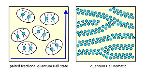
Image caption: Two different kinds of electron arrangements in a semiconductor, paired as composite particles or lined-up, can interact with and tweak each other in the presence of hydrostatic pressure. (Purdue University image/Gábor Csáthy)
What this means for semiconductor components, such as those that send information throughout electronic devices, is not yet clear, but hydrostatic pressure can be used to tune the interaction so that electrons paired as composite particles switch between paired, or "superconductor-like," and lined-up, or "nematic," phases. Forcing these phases to interact also suggests that they can influence each other's properties, like stability – opening up possibilities for manipulation in electronic devices and quantum computing.
"You can literally have hundreds of different phases of electrons organizing themselves in different ways in a semiconductor," said Gábor Csáthy, Purdue professor of physics and astronomy. "We found that two in particular can actually talk to each other in the presence of hydrostatic pressure."
Csáthy's group discovered that hydrostatic pressure, which is 10,000 times stronger than ambient pressure, compresses the lattice of atoms in a semiconductor and, therefore, influences the electron arrangement within a two-dimensional electron gas hosted by the semiconductor. The strength of the pressure determines which arrangement is favored and tunes the transition between the paired and lined-up phases, making them more tailorable for an application. Of the two phases, the paired phase may support a certain type of quantum computing.
"We can also tune the interaction by engineering the semiconductor," Csáthy said. "Say, for example, we grew a semiconductor with a particular width and electron density that we estimated could stabilize the nematic phase. Then we've tuned the electron-electron interaction as a result."
Michael Manfra, Purdue professor of physics and astronomy, electrical and computer engineering and materials engineering, and researchers Loren Pfeiffer and Kenneth West at Princeton University grew the semiconductor samples for this study. Yuli Lyanda-Geller, Purdue associate professor of physics and astronomy, provided theoretical support for the understanding on how these electron-electron interactions took place.
This research was supported by the U.S. Department of Energy, the National Science Foundation and various fellowships.
Share on:


Suggested Items
ZESTRON Academy Launches 2024 Advanced Packaging & Power Electronics Webinar Series
05/01/2024 | ZESTRONZESTRON, the leading global provider of high-precision cleaning products, services, and training solutions in the electronics manufacturing and semiconductor industries, proudly announces the launch of its highly anticipated webinar series on Advanced Packaging & Power Electronics, a webinar series on the latest innovations, cleaning, and corrosion challenges.
Worldwide Silicon Wafer Shipments Dip 5% in Q1 2024
05/01/2024 | SEMIWorldwide silicon wafer shipments decreased 5.4% quarter-over-quarter to 2,834 million square inches in the first quarter of 2024, a 13.2% drop from the 3,265 million square inches recorded during the same quarter last year, the SEMI Silicon Manufacturers Group (SMG) reported in its quarterly analysis of the silicon wafer industry.
Guerrilla RF Completes Strategic Acquisition of GaN Device Portfolio from Gallium Semiconductor
04/29/2024 | BUSINESS WIREGuerrilla RF, Inc. has finalized the acquisition of Gallium Semiconductor's entire portfolio of GaN power amplifiers and front-end modules. Effective April 26th, 2024, GUER acquired all previously released components as well as new cores under development at Gallium Semiconductor.
SIA Commends CHIPS Act Incentives for Micron’s Manufacturing Projects in New York and Idaho
04/29/2024 | SIAThe Semiconductor Industry Association (SIA) today released the following statement from SIA President and CEO John Neuffer applauding semiconductor manufacturing incentives announced by the U.S. Department of Commerce and Micron.
iNEMI Packaging Tech Topic Series: Role of EDA in Advanced Semiconductor Packaging
04/26/2024 | iNEMIAdvanced semiconductor packaging with heterogenous integration has made on-package integration of multiple chips a crucial part of finding alternatives to transistor scaling. Historically, EDA tools for front-end and back-end design have evolved separately; however, design complexity and the increased number of die-to-die or die-to-substrate interconnections has led to the need for EDA tools that can support integration of overall design planning, implementation, and system analysis in a single cockpit.