


 The Chemical Connection: Reducing Etch System Water Usage, Part 2
 It’s Only Common Sense: Nice Guys Really Can Finish First
 The Right Approach: I Hear the Train A Comin'
No Barrier to Applications for a Remarkable 2D Material
June 25, 2018 | A*STAREstimated reading time: 1 minute
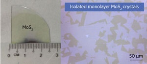
Mass production of large, uniform sheets of single-layer molybdenum disulfide, MoS2, is difficult, which limits its commercial application. A*STAR researchers have modified an existing manufacturing technique to enable the use of MoS2 in a range of technologies from photodevices to flexible, transparent sensors.
The two-dimensional material has attracted considerable attention because of its extraordinary physical, electronic and optoelectronic properties, including flexibility, transparency and semiconducting characteristics. But fabricating large-scale, defect-free single layers of MoS2 is highly challenging.
Dongzhi Chi and his team from the A*STAR Institute of Materials Research and Engineering, in collaboration with colleagues from the National University of Singapore and the Indian Institute of Science Education and Research, has modified a current technique, known as chemical vapor deposition (CVD), so that it can now produce uniform, centimeter-sized sheets of MoS2 crystals with large grain sizes.
“The physical properties of MoS2 vary greatly with its thickness,” explains Chi, “to maintain its remarkable electronic and physical properties we need a method that can uniformly deposit MoS2 films over a large area with high crystallinity.”
Although CVD is an effective technique for fabricating large-area, uniform sheets of MoS2 of varying thickness on different substrates, and significant progress has been made in improving the quality of MoS2 monolayers produced by the technique, little attention has been paid to controlling the chemical vapors using physical barriers during the growth of MoS2 crystals.
By introducing a nickel oxide (NiO) barrier, the researchers were able to control the concentration and distribution of chemical vapors during the growth of MoS2 crystals. Because NiO reacts with molybdenum trioxide (MoO3), one of the chemical reactants used in the growth process, it traps and lowers the MoO3 concentration, allowing the uniform deposition of monolayers of MoS2 over a large area.
“The advantage of this approach is the ease of implementation as well as a reduction in contamination, and it allows for control of the chemical exposure during the growth process,” says Chi.
The work has led to further advances in the fabrication of uniform and large-area MoS2 monolayers, and could also be applied to other two-dimensional materials.
“We are now looking to scale up our fabrication process for producing even larger sheets, which could pave the way for next-generation optoelectronic and sensor technologies,” says Chi.
Share on:


Suggested Items
Argonne, Toyota Collaborate on Cutting-Edge Battery Recycling Process
05/01/2024 | BUSINESS WIREThe U.S. Department of Energy’s (DOE) Argonne National Laboratory has recently launched a collaboration with Toyota Motor North America that could reduce the nation’s reliance on foreign sources of battery materials.
Real Time with… IPC APEX EXPO 2024: Outlining Rehm's Innovations and Global Presence
05/01/2024 | Real Time with...IPC APEX EXPOMichael Hanke, the chief sales officer for Rehm Thermal Systems, shares insights on the North American market, new machinery, and software development. He also discusses Rehm's turnkey solutions, process flexibility, global presence, and the dedicated team of 700 employees working on global solutions.
The Knowledge Base: A CM’s Perspective on Box Build Practices
04/30/2024 | Mike Konrad -- Column: The Knowledge BaseIn the ever-evolving landscape of electronics manufacturing, the box-build process stands out as a critical phase that bridges the gap between individual component manufacturing and the delivery of a fully functional electronic system. This intricate procedure, encompassing the assembly of everything from PCBs to wire harnesses and mechanical enclosures, demands a high level of precision, efficiency, and innovation. As the electronics assembly industry expands and diversifies, understanding the best practices within box-build assembly has become paramount for manufacturers aiming to stay ahead in a competitive market.
TSMC Certifies Ansys Multiphysics Platforms, Enabling Next-Gen AI and HPC Chips
04/30/2024 | PRNewswireAnsys announced the certification of its power integrity platforms for TSMC's N2 technology full production release. Both Ansys RedHawk-SC and Ansys Totem are certified for power integrity signoff on the N2 process, delivering significant speed and power advantages for high performance computing, mobile chips, and 3D-IC designs.
Koh Young Showcases Award-winning Inspection Solutions at SMTconnect with SmartRep in Hall 4A.225
04/25/2024 | Koh Young TechnologyKoh Young Technology, the industry leader in True 3D measurement-based inspection solutions, will showcase an array of award-winning inspection and measurement solutions at SMTconnect alongside its sales partner, SmartRep, in booth 4A.225 at NürnbergMesse from June 11-13, 2023. The following offers a glimpse into what Koh Young will present at the tradeshow: