


 Connect the Dots: Designing for the Future of Manufacturing Reality—Solder Mask and Legend
 Target Condition: An Exploration of Flooding PCB Layers
 Happy’s Tech Talk #47: Automation for Complex Multilayer Fabrication Stackups


iCD Introduces New Materials Planner Software
July 2, 2018 | ICDEstimated reading time: 1 minute
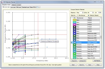
In-Circuit Design Pty Ltd (iCD), Australia, developer of the iCD Design Integrity software, has released the new iCD Materials Planner software to add to the Stackup Planner functionality. This will be rolled out to iCD support customers as an update to their current software.
The Dielectric Materials Library, which complements the iCD Stackup Planner, has
- Over 33,000 rigid and flexible materials up to 100GHz
- Produced by over 60 different manufacturers
- Containing over 700 series of materials
So, it is often a daunting task to ascertain which is the best material for an application. The iCD Materials Planner allows you to compare dielectric materials based on manufacturer, fabricator, frequency, dissipation factor (loss) and dielectric constant. This enables the designer to make an informed decision on which material is best for his application.
Generally the selection metric, for dielectric materials, is the amount of loss that a transmission line can tolerate and this is proportional to the frequency and rise time of the signals. The iCD Materials Planner is subdivided into five default TABs which gives the novice high-speed PCB designer a heads-up as to what to select for his application.
- Ultra Low Loss (Df ≤ 0.005)
- Low Loss (0.005 < Df < 0.010)
- Mid Loss (0.010 < Df < 0.015)
- Standard Loss (0.015 < Df < 0.02)
- Basic FR-4 (Df ≥ 0.02)
This is similar to a typical competitive analysis that a material manufacturer may present for, say, Isola vs Ventec and Rogers, but it is far more comprehensive, with over 60 vendors and 700 series of materials to choose from. Alternatively, a profile for each PCB fabricator that you usually deal with can be set up. This will display the complete range of materials that each Fab shop stocks ranging from basic FR-4 to low loss materials. This also enables the comparison of competitive Fab shop capabilities.
Watch below for a quick demonstration video of the iCD Materials Planner:
About In-Circuit Design Pty Ltd
In-Circuit Design Pty Ltd, based in Australia, developer of the iCD Design Integrity software incorporating the iCD Stackup, PDN and CPW Planner software, is a PCB Design Service Bureau and specialist in board level simulation. For further information or to download a free evaluation of the software, please click here.
Share on:


Testimonial
"Advertising in PCB007 Magazine has been a great way to showcase our bare board testers to the right audience. The I-Connect007 team makes the process smooth and professional. We’re proud to be featured in such a trusted publication."
Klaus Koziol - atgSuggested Items
FlashPCB Welcomes Adam Broeckert, EIT as Manufacturing Engineer
04/20/2026 | FlashPCBFlashPCB, a leading provider of quick-turn PCB assembly, is pleased to announce the addition of Adam Broeckert, EIT, as Manufacturing Engineer.
Single Pair Ethernet (SPE): A Valuable Option for Modern Designs
04/20/2026 | Marcy LaRont, I-Connect007When it comes to designing PCBs and full systems for increasingly complex electronics hardware, who doesn’t want to reduce complexity and cost? Single-Pair Ethernet (SPE) has emerged as a solution and is gaining rapid attention across industrial electronics and PCB design because it enables Ethernet communication over a single twisted pair, replacing the traditional two- or four-pair cabling used in standard Ethernet networks. This seemingly simple shift has significant implications for designers: smaller connectors, reduced cable weight, longer reach, and the ability to carry both data and power over a single pair.
DARPA Launches HARQ Program to Integrate Diverse Qubits for Scalable Quantum Computing
04/20/2026 | DARPADARPA has launched the Heterogeneous Architectures for Quantum (HARQ) program, an effort aimed at overcoming one of the most persistent barriers in quantum computing: how to move beyond single-technology systems to achieve and scale practical, high-impact applications.
Spirit Electronics Named Authorized Distributor for Microchip Technology
04/17/2026 | Globe NewswireSpirit Electronics, a vertically integrated electronics design and manufacturing solutions provider serving the military and aerospace markets, announced that it has been designated as an authorized distributor for the Americas for Microchip Technology, a broadline supplier of semiconductors committed to making innovative design easier through total system solutions.
Cadence, NVIDIA Expand AI & Accelerated Computing Partnership
04/17/2026 | Cadence Design Systems, Inc.At CadenceLIVE Silicon Valley 2026, Cadence announced an expanded partnership with NVIDIA to deliver accelerated solutions across agentic AI, physics-based simulation and digital twins to unlock new levels of productivity and accelerate next‑generation engineering design flows across semiconductor design, physical AI systems and hyperscale AI factories.