


 The Chemical Connection: Reducing Etch System Water Usage, Part 2
 It’s Only Common Sense: Nice Guys Really Can Finish First
 The Right Approach: I Hear the Train A Comin'
Electronic Stickers to Streamline Large-Scale 'Internet of Things'
July 17, 2018 | Purdue UniversityEstimated reading time: 2 minutes
Billions of objects ranging from smartphones and watches to buildings, machine parts and medical devices have become wireless sensors of their environments, expanding a network called the "Internet of Things."
As society moves toward connecting all objects to the internet – even furniture and office supplies – the technology that enables these objects to communicate and sense each other will need to scale up.
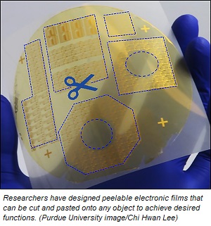
Researchers at Purdue University and the University of Virginia have developed a new fabrication method that makes tiny, thin-film electronic circuits peelable from a surface. The technique not only eliminates several manufacturing steps and the associated costs, but also allows any object to sense its environment or be controlled through the application of a high-tech sticker.
Eventually, these stickers could also facilitate wireless communication. The researchers demonstrate capabilities on various objects in a paper recently published in the Proceedings of the National Academy of Sciences.
"We could customize a sensor, stick it onto a drone, and send the drone to dangerous areas to detect gas leaks, for example," said Chi Hwan Lee, Purdue assistant professor of biomedical engineering and mechanical engineering.
*Most of today’s electronic circuits are individually built on their own silicon “wafer,” a flat and rigid substrate. The silicon wafer can then withstand the high temperatures and chemical etching that are used to remove the circuits from the wafer.
But high temperatures and etching damage the silicon wafer, forcing the manufacturing process to accommodate an entirely new wafer each time.
Lee’s new fabrication technique, called “transfer printing,” cuts down manufacturing costs by using a single wafer to build a nearly infinite number of thin films holding electronic circuits. Instead of high temperatures and chemicals, the film can peel off at room temperature with the energy-saving help of simply water.
“It’s like the red paint on San Francisco’s Golden Gate Bridge – paint peels because the environment is very wet,” Lee said. “So in our case, submerging the wafer and completed circuit in water significantly reduces the mechanical peeling stress and is environmentally friendly.”
A ductile metal layer, such as nickel, inserted between the electronic film and the silicon wafer, makes the peeling possible in water. These thin-film electronics can then be trimmed and pasted onto any surface, granting that object electronic features.
Putting one of the stickers on a flower pot, for example, made that flower pot capable of sensing temperature changes that could affect the plant’s growth.
Lee’s lab also demonstrated that the components of electronic integrated circuits work just as well before and after they were made into a thin film peeled from a silicon wafer. The researchers used one film to turn on and off an LED light display.
“We’ve optimized this process so that we can delaminate electronic films from wafers in a defect-free manner,” Lee said.
A YouTube video is available below:
Share on:


Suggested Items
iNEMI Names Grace O'Malley CTO
05/02/2024 | iNEMIThe Board of Directors of the International Electronics Manufacturing Initiative (iNEMI) has named Grace O'Malley Chief Technical Officer (CTO).
Intel Takes Next Step Toward Building Scalable Silicon-Based Quantum Processors
05/02/2024 | BUSINESS WIRENature published an Intel research paper, “Probing single electrons across 300-mm spin qubit wafers,” demonstrating state-of-the-art uniformity, fidelity and measurement statistics of spin qubits.
ZESTRON Academy Launches 2024 Advanced Packaging & Power Electronics Webinar Series
05/01/2024 | ZESTRONZESTRON, the leading global provider of high-precision cleaning products, services, and training solutions in the electronics manufacturing and semiconductor industries, proudly announces the launch of its highly anticipated webinar series on Advanced Packaging & Power Electronics, a webinar series on the latest innovations, cleaning, and corrosion challenges.
NextFlex Convenes the Hybrid Electronics Community at Binghamton University
05/01/2024 | NextFlexBinghamton University hosted the NextFlex hybrid electronics community on April 18 for a day of expert presentations, breakout sessions on technology and manufacturing topics, and networking.
HQ NextPCB of HQ Electronics Debut on the International Stage for Electronics Manufacture at IPC APEX 2024
05/01/2024 | PRNewswireHQ NextPCB of HQ Electronics, a leading Chinese-based multilayer PCB manufacturer and assembly house showcased its industrial prowess on the international stage for the first time at the IPC APEX Expo 2024.