


 The Right Approach: I Hear the Train A Comin'
 It’s Only Common Sense: OCCAM—the Time Is Now
 Marcy's Musings: The Growing Industry
Research Teams Selected to Uncover Novel Materials and Approaches to Circuit Integration
July 31, 2018 | DARPAEstimated reading time: 4 minutes
The use of intellectual-property (IP) blocks–discrete, modular, reusable blocks that deliver frequently used circuit functions—has significantly streamlined the design and creation of microchips. Just as the number of transistors per chip has grown dramatically in line with Moore’s Law—the transistor scaling that has allowed for 50 years of electronics advancement–so too has the number of IP blocks on those same chips. Finding ways of combining these dissimilar blocks, which often are composed of different materials and are comprised of different types of circuitry, into larger systems without affecting computational performance has been challenging for both the commercial and defense sectors.
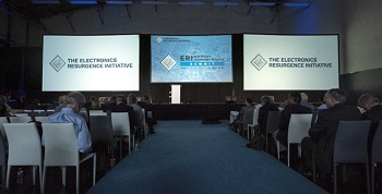
Image Caption: The three-day ERI Summit has brought together hundreds of members of the electronics community to explore the future of the industry and the impact this critical sector has on national defense. On July 23, attendees were the first to hear about the research teams selected to take on DARPA's six new ERI "Page 3" programs, which aim to jumpstart innovation across microelectronics design, architectures, and materials and integration.
Under DARPA’s Electronics Resurgence Initiative (ERI), research teams from academia and commercial industry have been selected to explore the roles new materials and radically different architectures can play in forming disparate chip components into larger systems. As a part of the ERI Materials & Integration research thrust area, DARPA has organized two programs–the Three Dimensional Monolithic System-on-a-Chip (3DSoC) program and the Foundations Required for Novel Compute (FRANC) program.
Yesterday, during the first annual DARPA ERI Summit in San Francisco, California, DARPA announced that a research team at the Georgia Institute of Technology and another team with researchers from Stanford University, Massachusetts Institute of Technology, and Skywater Technology Foundry will be working under the 3DSoC program. Meanwhile, HRL Laboratories; Applied Materials, Inc.; Ferric, Inc.; University of California, Los Angeles; University of Minnesota; and University of Illinois at Urbana-Champaign have been selected to take on the challenges of the FRANC program.
The three-day ERI Summit, which began on July 23, has brought together hundreds of members of the electronics community to explore the future of the industry and the impact this critical sector has on national defense.
Announced initially in September 2017, 3DSoC and FRANC are two of six ERI “Page 3” programs–so named for the way they map onto prescient guidance shared by Gordon Moore on the third page of his seminal 1965 research paper. In his paper, Moore envisioned building larger circuitry functions out of smaller functional blocks as a means of overcoming limitations to scaling in electronics. With this notion in mind, the ERI “Page 3” Materials & Integration programs seek to answer this question: Can we use the integration of unconventional electronics materials to enhance conventional silicon circuits and continue the progress in performance traditionally associated with scaling?
By setting researchers onto the task of investigating vertical, rather than flat or planar integration of microsystem components—as well as new materials, components, and algorithms capable of closing the gap between memory and logic functions—the program managers leading the 3DSoC and FRANC programs hope to create new means of computing vast amounts of information.
Today, electronic system performance is limited by the time and power required to access system memory—a restriction often referred to as the “memory bottleneck.” Integrating memory and logic into a single, monolithic 3D SoC stack has the potential to significantly reduce this constraint. The 3DSoC program aims to develop materials, design tools, and fabrication techniques for building microsystems on a single substrate with a third dimension. To achieve the program’s goals, 3DSoC research teams aim to integrate logic, memory, and input/output (I/O) elements in ways that dramatically shorten—more than 50-fold—computation times while using less power.
“Under the 3DSoC program, the researchers will build on a decade’s worth of theory and academic demonstration to integrate processes into a widely available foundry that should help, in practice, unleash these technologies in the field of microelectronics,” said Linton Salmon, the Microsystems Technology Office program manager leading 3DSoC.
To help further address the “memory bottleneck,” the second program under the ERI “Page 3” Materials & Integration research thrust area will explore alternatives to the conventional separation of memory and logic functions—a construct that falls under the category of von Neumann architectures. The time delay and energy expended in moving data between memory components that store it and processors that act on it are critical constraints on computer performance today. To address this challenge, the FRANC program seeks innovations that go beyond von Neumann compute architectures. Central here will be the design of circuits that leverage the properties of new materials and integration schemes to process data in ways that eliminate or minimize data movement. The novel compute topologies that come out of this effort could allow processing to happen where the data is stored with structures that are radically different from conventional digital logic processors, ultimately allowing for significant gains in compute performance.
“FRANC seeks to utilize new materials and devices to make 10x advances in embedded, non-volatile memories with the speed of static random access memory (SRAM) and the density of storage-class memory,” said Y.K. Chen, the Microsystems Technology Office program manager leading FRANC. “These advances could allow emerging memory-centric computing architectures to overcome the memory bottleneck presented in current von Neumann computing.”
ERI is a five-year, upwards of $1.5 billion investment to jumpstart innovation in the electronics industry. To address the impending engineering and economic challenges confronting those striving to push microelectronics technology forward, DARPA is nurturing research in circuit design tools, advanced new materials, and systems architectures through a mix of new and emerging programs. For more information about the Electronics Resurgence Initiative and the first annual ERI Summit, please click here.
Share on:


Suggested Items
Warm Windows and Streamlined Skin Patches – IDTechEx Explores Flexible and Printed Electronics
04/26/2024 | IDTechExFlexible and printed electronics can be integrated into cars and homes to create modern aesthetics that are beneficial and easy to use. From luminous car controls to food labels that communicate the quality of food, the uses of this technology are endless and can upgrade many areas of everyday life.
Book Excerpt: The Printed Circuit Assembler’s Guide to... Factory Analytics
04/24/2024 | I-Connect007 Editorial TeamIn our fast-changing, deeply competitive, and margin-tight industry, factory analytics can be the key to unlocking untapped improvements to guarantee a thriving business. On top of that, electronics manufacturers are facing a tremendous burden to do more with less. If you don't already have a copy of this book, what follows is an excerpt from the introduction chapter of 'The Printed Circuit Assembler’s Guide to... Factory Analytics: Unlocking Efficiency Through Data Insights' to whet your appetite.
Listen Up! The Intricacies of PCB Drilling Detailed in New Podcast Episode
04/25/2024 | I-Connect007In episode 5 of the podcast series, On the Line With: Designing for Reality, Nolan Johnson and Matt Stevenson continue down the manufacturing process, this time focusing on the post-lamination drilling process for PCBs. Matt and Nolan delve into the intricacies of the PCB drilling process, highlighting the importance of hole quality, drill parameters, and design optimization to ensure smooth manufacturing. The conversation covers topics such as drill bit sizes, aspect ratios, vias, challenges in drilling, and ways to enhance efficiency in the drilling department.
Elevating PCB Design Engineering With IPC Programs
04/24/2024 | Cory Blaylock, IPCIn a monumental stride for the electronics manufacturing industry, IPC has successfully championed the recognition of the PCB Design Engineer as an official occupation by the U.S. Department of Labor (DOL). This pivotal achievement not only underscores the critical role of PCB design engineers within the technology landscape, but also marks the beginning of a transformative journey toward nurturing a robust, skilled workforce ready to propel our industry into the future.
Winner of The Science Show Rakett 69 Receives Incap Scholarship
04/24/2024 | IncapThe winner of the Rakett 69 science show, Andri Türkson, who stood out as an electronics enthusiast, received a scholarship from Incap Estonia, along with an internship opportunity in Saaremaa.