


 It’s Only Common Sense: Nice Guys Really Can Finish First
 The Right Approach: I Hear the Train A Comin'
 Marcy's Musings: The Growing Industry
Scientists Create Biodegradable, Paper-Based Biobatteries
August 8, 2018 | Binghamton UniversityEstimated reading time: 1 minute
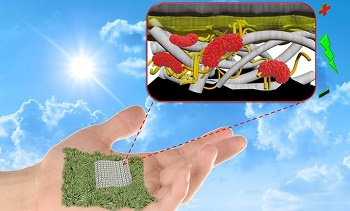
The batteries of the future may be made out of paper. Researchers at Binghamton University, State University at New York have created a biodegradable, paper-based battery that is more efficient than previously possible.
For years, there has been excitement in the scientific community about the possibility of paper-based batteries as an eco-friendly alternative. However, the proposed designs were never quite powerful enough, they were difficult to produce and it was questionable whether they were really biodegradable.
This new design solves all of those problems.
Associate Professor Seokheun "Sean" Choi from the Electrical and Computer Engineering Department and Professor Omowunmi Sadik from the Chemistry Department worked on the project together. Choi engineered the design of the paper-based battery, while Sadik was able to make the battery a self-sustaining biobattery.
"There's been a dramatic increase in electronic waste and this may be an excellent way to start reducing that," said Choi. "Our hybrid paper battery exhibited a much higher power-to-cost ratio than all previously reported paper-based microbial batteries."
The biobattery uses a hybrid of paper and engineered polymers. The polymers - poly (amic) acid and poly (pyromellitic dianhydride-p-phenylenediamine) - were the key to giving the batteries biodegrading properties. The team tested the degradation of the battery in water and it clearly biodegraded without the requirements of special facilities, conditions or introduction of other microorganisms.
The polymer-paper structures are lightweight, low-cost and flexible. Choi said that flexibility also provides another benefit.
"Power enhancement can be potentially achieved by simply folding or stacking the hybrid, flexible paper-polymer devices," said Choi.
The team said that producing the biobatteries is a fairly straightforward process and that the material allows for modifications depending on what configuration is needed.
Share on:


Suggested Items
iNEMI Packaging Tech Topic Series: Role of EDA in Advanced Semiconductor Packaging
04/26/2024 | iNEMIAdvanced semiconductor packaging with heterogenous integration has made on-package integration of multiple chips a crucial part of finding alternatives to transistor scaling. Historically, EDA tools for front-end and back-end design have evolved separately; however, design complexity and the increased number of die-to-die or die-to-substrate interconnections has led to the need for EDA tools that can support integration of overall design planning, implementation, and system analysis in a single cockpit.
Cadence, TSMC Collaborate on Wide-Ranging Innovations to Transform System and Semiconductor Design
04/25/2024 | Cadence Design SystemsCadence Design Systems, Inc. and TSMC have extended their longstanding collaboration by announcing a broad range of innovative technology advancements to accelerate design, including developments ranging from 3D-IC and advanced process nodes to design IP and photonics.
Ansys, TSMC Enable a Multiphysics Platform for Optics and Photonics, Addressing Needs of AI, HPC Silicon Systems
04/25/2024 | PRNewswireAnsys announced a collaboration with TSMC on multiphysics software for TSMC's Compact Universal Photonic Engines (COUPE). COUPE is a cutting-edge Silicon Photonics (SiPh) integration system and Co-Packaged Optics platform that mitigates coupling loss while significantly accelerating chip-to-chip and machine-to-machine communication.
Siemens’ Breakthrough Veloce CS Transforms Emulation and Prototyping with Three Novel Products
04/24/2024 | Siemens Digital Industries SoftwareSiemens Digital Industries Software launched the Veloce™ CS hardware-assisted verification and validation system. In a first for the EDA (Electronic Design Automation) industry, Veloce CS incorporates hardware emulation, enterprise prototyping and software prototyping and is built on two highly advanced integrated circuits (ICs) – Siemens’ new, purpose-built Crystal accelerator chip for emulation and the AMD Versal™ Premium VP1902 FPGA adaptive SoC (System-on-a-chip) for enterprise and software prototyping.
Listen Up! The Intricacies of PCB Drilling Detailed in New Podcast Episode
04/25/2024 | I-Connect007In episode 5 of the podcast series, On the Line With: Designing for Reality, Nolan Johnson and Matt Stevenson continue down the manufacturing process, this time focusing on the post-lamination drilling process for PCBs. Matt and Nolan delve into the intricacies of the PCB drilling process, highlighting the importance of hole quality, drill parameters, and design optimization to ensure smooth manufacturing. The conversation covers topics such as drill bit sizes, aspect ratios, vias, challenges in drilling, and ways to enhance efficiency in the drilling department.