-

- News
- Books
Featured Books
- design007 Magazine
Latest Issues
Current Issue
Proper Floor Planning
Floor planning decisions can make or break performance, manufacturability, and timelines. This month’s contributors weigh in with their best practices for proper floor planning and specific strategies to get it right.

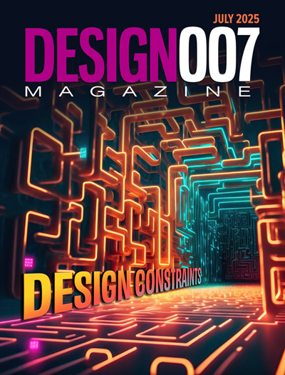
Showing Some Constraint
A strong design constraint strategy carefully balances a wide range of electrical and manufacturing trade-offs. This month, we explore the key requirements, common challenges, and best practices behind building an effective constraint strategy.

All About That Route
Most designers favor manual routing, but today's interactive autorouters may be changing designers' minds by allowing users more direct control. In this issue, our expert contributors discuss a variety of manual and autorouting strategies.
- Articles
- Columns
- Links
- Media kit
||| MENU - design007 Magazine
The Impact of PCB Dielectric Thickness on Signal Crosstalk
August 27, 2018 | Chang Fei Yee, Keysight TechnologiesEstimated reading time: Less than a minute
This article studies the impact of dielectric thickness on crosstalk for transmission lines in single-ended and differential mode on outer (microstrip) and inner (stripline) PCB layers. Crosstalk analysis is performed in 2D simulation and S-parameters are subsequently observed.
Introduction to Crosstalk
Crosstalk is an unintentional electromagnetic (EM) field coupling between transmission lines on a PCB. This phenomenon becomes a major culprit in signal integrity (SI), contributing to the rise of bit error occurrence in data communications and electromagnetic interference (EMI). With the existence of mutual inductance and capacitance between two adjacent transmission lines on a PCB, crosstalk has become more severe due to the shorter signal rise/fall times at today’s higher data speed rates.
Crosstalk can be minimized by routing the PCB traces further apart and reducing the dielectric thickness between PCB trace and reference plane. We will observe how a PCB’s dielectric thickness affects the signal crosstalk. All crosstalk analyses are carried out in 2D simulation using Mentor’s HyperLynx.
To read this entire article, which appeared in the August 2018 issue of Design007 Magazine, click here.
Testimonial
"The I-Connect007 team is outstanding—kind, responsive, and a true marketing partner. Their design team created fresh, eye-catching ads, and their editorial support polished our content to let our brand shine. Thank you all! "
Sweeney Ng - CEE PCBSuggested Items
Walt Custer: Making Data Interesting
09/03/2025 | Andy Shaughnessy, I-Connect007I just learned that IPC Hall of Famer Walt Custer has passed away at 81. I first met Walt about 20 years ago when I started covering the fabrication industry. Right away, he started telling me which companies to watch and which trends to follow. This was in the years following 9/11, and things were still pretty fluid.
Altus Supports Datalink Electronics with Advanced Selective Soldering Solution to Boost Manufacturing Efficiency
09/02/2025 | Altus GroupDatalink Electronics has partnered with Altus Group to integrate a cutting-edge automated soldering solution, enhancing its production capabilities and reinforcing its strategic focus on quality, automation, and scalability.
Wisdom From Data-center Power Pioneer Mike Mosman
09/02/2025 | Barry Matties, I-Connect007Few engineers have moved the levers of modern electronics more decisively than Mike Mosman. From the pre-email computer rooms of the 1980s to today’s hyperscale campuses cranking out AI cycles, the retired power engineer and co-founder of CCG Facilities Integration has spent four decades proving that uptime is a design discipline, not a hope.
HPE Accelerates Self-driving Network Operations with New Mist Agentic AI-native Innovations
08/26/2025 | BUSINESS WIREHPE announced major innovations to its HPE Juniper Networking portfolio, advancing its AI-native Mist platform to deliver agentic AIOps through more autonomous, intelligent and proactive network operations.
Macronix Introduces Cutting-Edge Secure-Boot NOR Flash Memory
08/08/2025 | PRNewswireMacronix International Co., Ltd., a leading integrated device manufacturer in the non-volatile memory (NVM) market, announced ArmorBoot MX76, a robust NOR flash memory combining in a single device, the essential performance and an array of security features that deliver rapid boot times and iron-clad data protection.


