


 It’s Only Common Sense: Nice Guys Really Can Finish First
 The Right Approach: I Hear the Train A Comin'
 Marcy's Musings: The Growing Industry
New NIST Method Measures 3D Polymer Processing Precisely
October 9, 2018 | NISTEstimated reading time: 2 minutes
Recipes for three-dimensional (3D) printing, or additive manufacturing, of parts have required as much guesswork as science. Until now.
Resins and other materials that react under light to form polymers, or long chains of molecules, are attractive for 3D printing of parts ranging from architectural models to functioning human organs. But it’s been a mystery what happens to the materials’ mechanical and flow properties during the curing process at the scale of a single voxel. A voxel is a 3D unit of volume, the equivalent of a pixel in a photo.
Now, researchers at the National Institute of Standards and Technology (NIST) have demonstrated a novel light-based atomic force microscopy (AFM) technique—sample-coupled-resonance photorheology (SCRPR)—that measures how and where a material’s properties change in real time at the smallest scales during the curing process.
“We have had a ton of interest in the method from industry, just as a result of a few conference talks,” NIST materials research engineer Jason Killgore said. He and his colleagues have now published the technique in the journal Small Methods.
3D printing, or additive manufacturing, is lauded for flexible, efficient production of complex parts but has the disadvantage of introducing microscopic variations in a material’s properties. Because software renders the parts as thin layers and then reconstructs them in 3D before printing, the physical material’s bulk properties no longer match those of the printed parts. Instead, the performance of fabricated parts depends on printing conditions.
NIST’s new method measures how materials evolve with submicrometer spatial resolution and submillisecond time resolution—thousands of times smaller-scale and faster than bulk measurement techniques. Researchers can use SCRPR to measure changes throughout a cure, collecting critical data for optimizing processing of materials ranging from biological gels to stiff resins.
The new method combines AFM with stereolithography, the use of light to pattern photo-reactive materials ranging from hydrogels to reinforced acrylics. A printed voxel may turn out uneven due to variations in light intensity or the diffusion of reactive molecules.
AFM can sense rapid, minute changes in surfaces. In the NIST SCRPR method, the AFM probe is continuously in contact with the sample. The researchers adapted a commercial AFM to use an ultraviolet laser to start the formation of the polymer (“polymerization”) at or near the point where the AFM probe contacts the sample.
The method measures two values at one location in space during a finite timespan. Specifically, it measures the resonance frequency (the frequency of maximum vibration) and quality factor (an indicator of energy dissipation) of the AFM probe, tracking changes in these values throughout the polymerization process. These data can then be analyzed with mathematical models to determine material properties such as stiffness and damping.
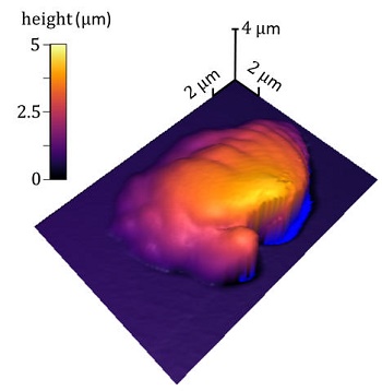
The method was demonstrated with two materials. One was a polymer film transformed by light from a rubber into a glass. Researchers found that the curing process and properties depended on exposure power and time and were spatially complex, confirming the need for fast, high-resolution measurements. The second material was a commercial 3D printing resin that changed from liquid into solid form in 12 milliseconds. A rise in resonance frequency seemed to signal polymerization and increased elasticity of the curing resin. Therefore, researchers used the AFM to make topographic images of a single polymerized voxel.
Surprising the researchers, interest in the NIST technique has extended well beyond the initial 3D printing applications. Companies in the coatings, optics and additive manufacturing fields have reached out, and some are pursing formal collaborations, NIST researchers say.
Share on:


Suggested Items
Indium Corporation Expert to Present on Pb-Free Solder for Die-Attach in Discrete Power Applications
04/30/2024 | Indium CorporationIndium Corporation Product Manager – Semiconductor Dean Payne will present at the Advanced Packaging for Power Electronics conference, hosted by IMAPS, held May 8-9 in Woburn, Massachusetts, USA.
Real Time with... IPC APEX EXPO 2024: Adhesive Materials and Equipment Update with Dymax
05/01/2024 | Real Time with...IPC APEX EXPOVirginia Hogan, global business development manager at Dymax, discusses adhesive materials, dispensing and curing equipment, a new, high-reliability conformal coating, and various materials and dispensing methods.
Real Time with... IPC APEX EXPO 2024: Sustainability in the Industry
04/26/2024 | Real Time with...IPC APEX EXPOGuest Editor Henry Crandall and Chris Nash of Indium Corporation discuss the company's 90th anniversary and its focus on sustainability. They focus on the benefits of sustainable materials, their compatibility, and value propositions. The conversation also highlights how Durafuse LT technology's role in reducing reflow temperatures is leading to significant cost and energy savings. Nash also touches on downstream sustainability efforts such as using recycled materials for packaging.
SMC Korea 2024 to Highlight Semiconductor Materials Trends and Innovations on Industry’s Path to $1 Trillion
04/24/2024 | SEMIWith Korea a major consumer of semiconductor materials and advanced materials a key driver of innovation on the industry’s path to $1 trillion, industry leaders and experts will gather at SMC (Strategic Materials Conference) Korea 2024 on May 29 at the Suwon Convention Center in Gyeonggi-do, South Korea to provide insights into the latest materials developments and trends. Registration is open.
Groundbreaking Ceremony Marks the Beginning of a New Era for Newccess Industrial; The Construction of the MINGXIN Building
04/12/2024 | Newccess IndustrialOn a clear and sunny day in March, the groundbreaking ceremony for the MINGXIN Building took place in Shenzhen, China. This moment marked the official commencement of construction for a project that will reshape the semiconductor materials industry.