


 It’s Only Common Sense: Nice Guys Really Can Finish First
 The Right Approach: I Hear the Train A Comin'
 Marcy's Musings: The Growing Industry
Draw-Your-Own Electrodes Set to Speed up Development of Micro Detection Devices
November 12, 2018 | Imperial College LondonEstimated reading time: 2 minutes
Miniature devices for sensing biological molecules could be developed more quickly thanks to a rapid prototyping method.
Devices that sense and measure biological molecules important for healthcare, such as detecting diseases in blood samples, rely on electrodes to carry out their tasks.
We hope this method will allow bioelectronics to benefit from that ecosystem of hackers getting hands-on with problems and solutions in healthcare.
New generations of these devices are being made that manipulate molecules or work with smaller concentrations of molecules, for example detecting rare cancer cells in blood samples.
These require intricate patterning of minute electrodes. Getting the right pattern is key, but building prototypes of different electrode designs can be expensive and time-consuming, often requiring specialist equipment and expertise.
Now, researchers at Imperial College London, have created a method that allows intricate electrode patterns to be printed in community labs and hackspaces at a fraction of the time and cost. The details of their method are published in Scientific Reports.
Democratising Science
Lead researcher Dr Ali Salehi-Reyhani, from the Department of Chemistry at Imperial, said: “With our method researchers and startups can more easily design and develop analytical devices, even when they need electronics that can’t be bought off-the-shelf.
“Community hackspaces are great for democratising science, allowing more people to try out new technology solutions. We hope this method will allow bioelectronics to benefit from that ecosystem of hackers getting hands-on with problems and solutions in healthcare.”
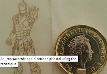
The method allows researchers to design electrode patterns on computers before printing them off using a laser-cutting printer. The cavities are then filled with metal using microfluidic techniques—using the science of how fluids move through confined spaces.
In this way, researchers could print several sheets of electrodes, each with a slightly different design, allowing them to be tested in rapid succession to find the best design. Previously, designs may have had to be sent away to be manufactured, taking weeks or even months to arrive at the best design, but now the whole process can be reduced to a matter of days.
Manipulating and Analyzing Cells
The team at fabriCELL, a centre of excellence in artificial cell science run by Imperial College London and King’s College London, are now using the technique to prototype devices for manipulating and analysing cells.
They say the technique could be used to speed up the development of flexible wearable devices, such as skin patches that monitor health signals and devices, and devices that could be used in hospitals or GP surgeries, such as ones that can quickly distinguish between viral and bacterial infections with just a drop of blood.
Share on:


Suggested Items
Real Time with… IPC APEX EXPO 2024: Ventec Discusses New Pro-bond Family of Advanced Products
05/01/2024 | Real Time with...IPC APEX EXPOChris Hanson, Ventec's Global Head of IMS Technology, outlines the launch of four pro-bond formulas that deliver an outstanding combination of low dissipation factor (Df) with a dielectric constant (Dk) range to maximize the design window for critical PCB parameters. As Chris points out, Pro-bond is designed for low-loss, high-speed applications, while thermal-bond dissipates heat from a component through the board to a heat sink.
IPC's Vision for Empowering PCB Design Engineers
04/30/2024 | Robert Erickson, IPCAs architects of innovation, printed circuit board designers are tasked with translating increasingly complex concepts into tangible designs that power our modern world. IPC provides the necessary community, standards framework, and education to prepare these pioneers as they explore the boundaries of what’s possible, equipping engineers with the knowledge, skills, and resources required to thrive in an increasingly dynamic field.
iNEMI Packaging Tech Topic Series: Role of EDA in Advanced Semiconductor Packaging
04/26/2024 | iNEMIAdvanced semiconductor packaging with heterogenous integration has made on-package integration of multiple chips a crucial part of finding alternatives to transistor scaling. Historically, EDA tools for front-end and back-end design have evolved separately; however, design complexity and the increased number of die-to-die or die-to-substrate interconnections has led to the need for EDA tools that can support integration of overall design planning, implementation, and system analysis in a single cockpit.
Cadence, TSMC Collaborate on Wide-Ranging Innovations to Transform System and Semiconductor Design
04/25/2024 | Cadence Design SystemsCadence Design Systems, Inc. and TSMC have extended their longstanding collaboration by announcing a broad range of innovative technology advancements to accelerate design, including developments ranging from 3D-IC and advanced process nodes to design IP and photonics.
Ansys, TSMC Enable a Multiphysics Platform for Optics and Photonics, Addressing Needs of AI, HPC Silicon Systems
04/25/2024 | PRNewswireAnsys announced a collaboration with TSMC on multiphysics software for TSMC's Compact Universal Photonic Engines (COUPE). COUPE is a cutting-edge Silicon Photonics (SiPh) integration system and Co-Packaged Optics platform that mitigates coupling loss while significantly accelerating chip-to-chip and machine-to-machine communication.