-

-
News
News Highlights
- Books
Featured Books
- design007 Magazine
Latest Issues
Current Issue
All About That Route
Most designers favor manual routing, but today's interactive autorouters may be changing designers' minds by allowing users more direct control. In this issue, our expert contributors discuss a variety of manual and autorouting strategies.

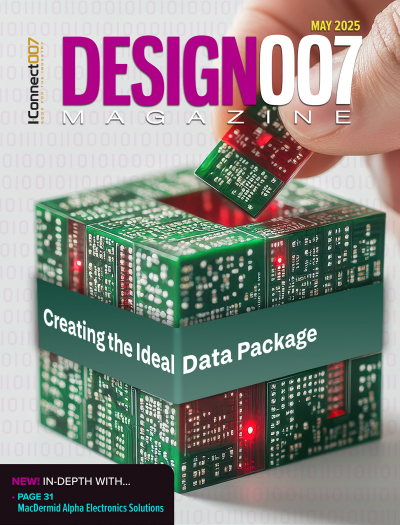
Creating the Ideal Data Package
Why is it so difficult to create the ideal data package? Many of these simple errors can be alleviated by paying attention to detail—and knowing what issues to look out for. So, this month, our experts weigh in on the best practices for creating the ideal design data package for your design.

Designing Through the Noise
Our experts discuss the constantly evolving world of RF design, including the many tradeoffs, material considerations, and design tips and techniques that designers and design engineers need to know to succeed in this high-frequency realm.
- Articles
- Columns
- Links
- Media kit
||| MENU - design007 Magazine
Ventec's Technology Ambassador Alun Morgan to Keynote at AltiumLive 2019
January 14, 2019 | Ventec International GroupEstimated reading time: 1 minute
Ventec International Group Co., Ltd., a world leader in the production of polyimide and high reliability epoxy laminates and prepregs and specialist provider of thermal management and IMS solutions, is pleased to announce Technology Ambassador Alun Morgan as a keynote speaker at the AltiumLive summit in Munich on the 16 January 2019 with a presentation on ‘PCB base material properties and developments: What designers need to know'.
AltiumLive is the annual PCB design summit which has quickly become one of the largest electronics conferences in the world.
Alun's presentation will focus on PCB base material properties and developments, aiming to give designers a greater understanding of the base materials used in their designs and the critical properties of base materials that impact performance.
Alun will review the development of high reliability base materials for PCBs with a focus on thermal performance, reliability and signal integrity. He will explore classification by application as a method of substrate selection which gives the designer the flexibility to select the appropriate substrate for an application without over engineering performance that is neither required nor can be afforded. The presentation includes a straightforward guide to the PCB substrate manufacturing process emphasising the impact of resin chemistry, material reinforcement and copper foil properties on substrate performance. Armed with this knowledge, PCB Designers will be able to better specify and choose appropriate materials for their needs.
Ian Mayoh, European technical support manager, will also be expertly on hand throughout the event and at the Ventec booth for any technical advice required.
About Ventec International Group
Ventec International is a premier supplier to the Global PCB industry. With volume manufacturing facilities in Taiwan and China and distribution locations and manufacturing sites in both the US and Europe, Ventec specializes in advanced copper clad glass reinforced and metal backed substrates. Ventec materials, which include high-quality enhanced FR4, high-speed/low-loss- & high-performance IMS material technology and an advanced range of thermal management solutions, are manufactured by Ventec using strict quality-controlled processes that are certified to AS9100 Revision D, IATF 16949:2016 and ISO 9001:2015, and are backed by a fully controlled and managed global supply chain, sales- and technical support-network.
Visit I-007eBooks to download your copy of Ventec micro eBook today:
The Printed Circuit Designer's Guide to...Thermal Management with Insulated Metal Substrates
Suggested Items
The Evolution of Picosecond Laser Drilling
06/19/2025 | Marcy LaRont, PCB007 MagazineIs it hard to imagine a single laser pulse reduced not only from nanoseconds to picoseconds in its pulse duration, but even to femtoseconds? Well, buckle up because it seems we are there. In this interview, Dr. Stefan Rung, technical director of laser machines at Schmoll Maschinen GmbH, traces the technology trajectory of the laser drill from the CO2 laser to cutting-edge picosecond and hybrid laser drilling systems, highlighting the benefits and limitations of each method, and demonstrating how laser innovations are shaping the future of PCB fabrication.
Day 2: More Cutting-edge Insights at the EIPC Summer Conference
06/18/2025 | Pete Starkey, I-Connect007The European Institute for the PCB Community (EIPC) summer conference took place this year in Edinburgh, Scotland, June 3-4. This is the third of three articles on the conference. The other two cover Day 1’s sessions and the opening keynote speech. Below is a recap of the second day’s sessions.
Day 1: Cutting Edge Insights at the EIPC Summer Conference
06/17/2025 | Pete Starkey, I-Connect007The European Institute for the PCB Community (EIPC) Summer Conference took place this year in Edinburgh, Scotland, June 3-4. This is the second of three articles on the conference. The other two cover the keynote speeches and Day 2 of the technical conference. Below is a recap of the first day’s sessions.
Preventing Surface Prep Defects and Ensuring Reliability
06/10/2025 | Marcy LaRont, PCB007 MagazineIn printed circuit board (PCB) fabrication, surface preparation is a critical process that ensures strong adhesion, reliable plating, and long-term product performance. Without proper surface treatment, manufacturers may encounter defects such as delamination, poor solder mask adhesion, and plating failures. This article examines key surface preparation techniques, common defects resulting from improper processes, and real-world case studies that illustrate best practices.
RF PCB Design Tips and Tricks
05/08/2025 | Cherie Litson, EPTAC MIT CID/CID+There are many great books, videos, and information online about designing PCBs for RF circuits. A few of my favorite RF sources are Hans Rosenberg, Stephen Chavez, and Rick Hartley, but there are many more. These PCB design engineers have a very good perspective on what it takes to take an RF design from schematic concept to PCB layout.


