


 The Right Approach: I Hear the Train A Comin'
 It’s Only Common Sense: OCCAM—the Time Is Now
 Marcy's Musings: The Growing Industry
Neurocomputing Lab Creates First Russian Neural Network Processor
February 7, 2019 | MIPTEstimated reading time: 2 minutes
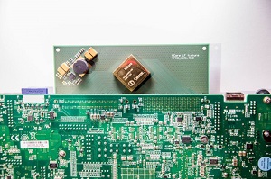
Engineers and researchers working under a project of the Russian Foundation for Advanced Research (FAR) — a government agency for defense research — has demonstrated the first Russian-made specialized neural network processor for energy efficient execution of machine learning algorithms based on deep neural networks. These algorithms are widely used to automatically solve tasks in image and speech recognition, self-driving car control, and elsewhere. The prime contractor of the project is the Neurocomputing Systems Lab of the Moscow Institute of Physics and Technology.
Machine learning algorithms that rely on deep neural networks require considerable computing power, and they are typically run using graphics accelerators. The latter consume way too much power to be of use on a mobile platform, such as small unmanned aerial or ground vehicles or smart cameras. This is why researchers worldwide are pursuing the notion of specialized neural network tensor processors. By leveraging certain computing capabilities of neural networks, tensor processing units can achieve a much higher energy efficiency, compared with graphics accelerators.
MIPT has demonstrated NCore, a neural network processor created under the 65-nanometer design standard. Although the processor was manufactured outside Russia, the required technology is currently being introduced at a Mikron facility in Zelenograd, a suburb of Moscow. NCore achieves an energy efficiency comparable to that of graphics accelerators complying with the more advanced 28-nanometer design standard or even stricter guidelines.
According to Alexey Zablotskiy, who heads the FAR project group, the architecture can be scaled down to create Russian neural network processors under “thinner” design standards. This would ensure scientific and technological parity in specialized tensor processing unit design for machine learning algorithms, Zablotskiy added.
“By now we have developed the basic elements: processor cores, interfaces, and the essential software,” said Dmitriy Negrov from the MIPT Neurocomputing Systems Lab. “Our software for algorithm translation enables us to convert a neural network to launch it with our system using popular machine learning frameworks.”
“We already have a system prototype in silicon, manufactured using the 65-nanometer technology, which is fairly coarse by modern standards. Eventually we intend to use our cores as components for crystal-based systems,” the researcher added.
An important part of the project is developing an automated translator for machine learning algorithms developed using the popular frameworks TensorFlow, Caffe, and Keras. This unification will enable users to work in familiar environments.
NCore testing with prospective consumer participation is scheduled for spring 2019. Following this, an improved version of the processor will be created.
Project co-contractors alongside the MIPT lab include the State Research Institute for Aviation Systems and the Bruk Institute of Electronic Control Machines. The project is supported by the Russian Ministry of Education and Science
Share on:


Suggested Items
iNEMI Packaging Tech Topic Series: Role of EDA in Advanced Semiconductor Packaging
04/26/2024 | iNEMIAdvanced semiconductor packaging with heterogenous integration has made on-package integration of multiple chips a crucial part of finding alternatives to transistor scaling. Historically, EDA tools for front-end and back-end design have evolved separately; however, design complexity and the increased number of die-to-die or die-to-substrate interconnections has led to the need for EDA tools that can support integration of overall design planning, implementation, and system analysis in a single cockpit.
Cadence, TSMC Collaborate on Wide-Ranging Innovations to Transform System and Semiconductor Design
04/25/2024 | Cadence Design SystemsCadence Design Systems, Inc. and TSMC have extended their longstanding collaboration by announcing a broad range of innovative technology advancements to accelerate design, including developments ranging from 3D-IC and advanced process nodes to design IP and photonics.
Ansys, TSMC Enable a Multiphysics Platform for Optics and Photonics, Addressing Needs of AI, HPC Silicon Systems
04/25/2024 | PRNewswireAnsys announced a collaboration with TSMC on multiphysics software for TSMC's Compact Universal Photonic Engines (COUPE). COUPE is a cutting-edge Silicon Photonics (SiPh) integration system and Co-Packaged Optics platform that mitigates coupling loss while significantly accelerating chip-to-chip and machine-to-machine communication.
Siemens’ Breakthrough Veloce CS Transforms Emulation and Prototyping with Three Novel Products
04/24/2024 | Siemens Digital Industries SoftwareSiemens Digital Industries Software launched the Veloce™ CS hardware-assisted verification and validation system. In a first for the EDA (Electronic Design Automation) industry, Veloce CS incorporates hardware emulation, enterprise prototyping and software prototyping and is built on two highly advanced integrated circuits (ICs) – Siemens’ new, purpose-built Crystal accelerator chip for emulation and the AMD Versal™ Premium VP1902 FPGA adaptive SoC (System-on-a-chip) for enterprise and software prototyping.
Listen Up! The Intricacies of PCB Drilling Detailed in New Podcast Episode
04/25/2024 | I-Connect007In episode 5 of the podcast series, On the Line With: Designing for Reality, Nolan Johnson and Matt Stevenson continue down the manufacturing process, this time focusing on the post-lamination drilling process for PCBs. Matt and Nolan delve into the intricacies of the PCB drilling process, highlighting the importance of hole quality, drill parameters, and design optimization to ensure smooth manufacturing. The conversation covers topics such as drill bit sizes, aspect ratios, vias, challenges in drilling, and ways to enhance efficiency in the drilling department.