


 The Right Approach: I Hear the Train A Comin'
 It’s Only Common Sense: OCCAM—the Time Is Now
 Marcy's Musings: The Growing Industry
Graphene and Boron Nitride ‘Sandwich’ Key to New Electronics
February 19, 2019 | Graphene FlagshipEstimated reading time: 3 minutes
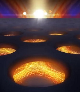
Since its inception, scientists have tried to exploit graphene to produce nano-sized electronics. However, since graphene is only an atom thick, all atoms are exposed to the outside world, and even small amounts of defects and impurities impede its properties. Now, Graphene Flagship researchers at DTU, Denmark solved this problem by protecting graphene with insulating layers of hexagonal boron nitride, another two-dimensional material with insulating properties.
Peter Bøggild, researcher at Graphene Flagship partner DTU and coauthor of the paper, explains that although "graphene is a fantastic material that could play a crucial role in making new nano-sized electronics, it is still extremely difficult to control its electrical properties." Since 2010, scientists at DTU have tried to tailor the electrical properties of graphene, by making a very fine pattern of holes, so that channels through which an electric power can flow freely are formed.
"Creating nanostructured graphene turned out to be amazingly difficult, since even small errors wash out all the properties we designed it to have," comments Bøggild.
Now, researchers from Graphene Flagship partner DTU made a leap forward. Bjarke Jessen and Lene Gammelgaard encapsulated graphene with another 2D material, hexagonal boron nitride, which is very similar to graphene, but electrically insulating. Then, using nanolithography, they carefully drilled nanoscopic holes in graphene through the protective layer of boron nitride. The holes have a diameter of approximately 20 nanometers, and are separated from each other with just 12 nanometers. This great precision makes possible to send an electrical current through the graphene that is 100-1000 times higher than typical numbers for lithographically carved nanographene.
"When you make patterns in a material like graphene, you do so in order to change its properties. However, what we have seen throughout the years is that when we shape graphene on this fine scale, it does not behave like graphene anymore - there is too much disorder,’ explains Bøggild. ‘Many scientists have abandoned nanolithography in graphene on this scale, but now we have figured out how it can be done - you could say that the curse is lifted," he adds.
"We have shown that we can control graphene’s band structure and that deterministic design of nanoelectronics is realistic. Looking solely at electronics, this means that we can make insulators, transistors, conductors and perhaps even superconductors, as our nanolithography can preserve the subtle inter-layer physics that was recently shown to lead to superconductivity in double-layer graphene. However, it goes way beyond that. When we control the band structure, we have access to all of graphene’s properties. In other words, we could sit in front of the computer and dream up other applications - and then go to the laboratory and make them happen," says Bøggild. ‘There are plenty of practical challenges, but the fact that we can tailor electronic properties of graphene is a big step towards creating new electronics with extremely small dimensions,’ he concludes.
Daniel Neumaier, Graphene Flagship Division Leader for Electronics and Photonics Integration says: ‘Controlling the electronic properties of graphene by nano-pattering offers an additional degree of freedom for the design of electronic and photonic devices, which was so far not accessible. The researchers from Graphene Flagship partner DTU and their co-workers now discovered a unique way for nano-patterning of graphene without seeing the limitations of patterning introduced defects. This was the key enabling step for using the nano-patterning induced electronic properties of graphene in real device and we are expecting significant advances especially for nano-electronics and photonics based on these results.’
Andrea C. Ferrari, Science and Technology Officer of the Graphene Flagship and Chair of its Management Panel added how "patterning of graphene to create nano-electronic devices was one of the first approaches attempted to exploit this unique material into devices. However, after an initial flurry of publications, the amount of damage produced was so much that this line of research was almost entirely abandoned. The work presented here shows how the long term nature of the Flagship allows scientists to pursue and solve even apparently intractable problems. This will rejuvenate the interest in graphene nanoelectronics, and could lead to a variety of useful devices, previously hampered by defects."
Share on:


Suggested Items
Warm Windows and Streamlined Skin Patches – IDTechEx Explores Flexible and Printed Electronics
04/26/2024 | IDTechExFlexible and printed electronics can be integrated into cars and homes to create modern aesthetics that are beneficial and easy to use. From luminous car controls to food labels that communicate the quality of food, the uses of this technology are endless and can upgrade many areas of everyday life.
Book Excerpt: The Printed Circuit Assembler’s Guide to... Factory Analytics
04/24/2024 | I-Connect007 Editorial TeamIn our fast-changing, deeply competitive, and margin-tight industry, factory analytics can be the key to unlocking untapped improvements to guarantee a thriving business. On top of that, electronics manufacturers are facing a tremendous burden to do more with less. If you don't already have a copy of this book, what follows is an excerpt from the introduction chapter of 'The Printed Circuit Assembler’s Guide to... Factory Analytics: Unlocking Efficiency Through Data Insights' to whet your appetite.
Listen Up! The Intricacies of PCB Drilling Detailed in New Podcast Episode
04/25/2024 | I-Connect007In episode 5 of the podcast series, On the Line With: Designing for Reality, Nolan Johnson and Matt Stevenson continue down the manufacturing process, this time focusing on the post-lamination drilling process for PCBs. Matt and Nolan delve into the intricacies of the PCB drilling process, highlighting the importance of hole quality, drill parameters, and design optimization to ensure smooth manufacturing. The conversation covers topics such as drill bit sizes, aspect ratios, vias, challenges in drilling, and ways to enhance efficiency in the drilling department.
Elevating PCB Design Engineering With IPC Programs
04/24/2024 | Cory Blaylock, IPCIn a monumental stride for the electronics manufacturing industry, IPC has successfully championed the recognition of the PCB Design Engineer as an official occupation by the U.S. Department of Labor (DOL). This pivotal achievement not only underscores the critical role of PCB design engineers within the technology landscape, but also marks the beginning of a transformative journey toward nurturing a robust, skilled workforce ready to propel our industry into the future.
Winner of The Science Show Rakett 69 Receives Incap Scholarship
04/24/2024 | IncapThe winner of the Rakett 69 science show, Andri Türkson, who stood out as an electronics enthusiast, received a scholarship from Incap Estonia, along with an internship opportunity in Saaremaa.