


 The Right Approach: I Hear the Train A Comin'
 It’s Only Common Sense: OCCAM—the Time Is Now
 Marcy's Musings: The Growing Industry
Argonne Takes the Guesswork out of Electrospinning
May 29, 2019 | Argonne National LaboratoryEstimated reading time: 3 minutes
Capturing real-time data as nanofibers form makes the technique more affordable and effective.
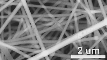
Electrospun fibers have a high surface-area-to-volume ratio, which favors surface reaction applications like catalysts, and superior mechanical properties compared with their bulk counter parts, making them less subject to mechanical failure.
Image Caption: Electrospun fibers have a high surface-area-to-volume ratio, which favors surface reaction applications like catalysts, and superior mechanical properties compared with their bulk counterparts, making them less subject to mechanical failure.
Electrospinning, a nanofiber fabrication method, can produce nanometer- to micrometer-diameter ceramic, polymer, and metallic fibers of various compositions for a wide spectrum of applications: tissue engineering, filtration, fuel cells and lithium batteries. These materials have unique properties because of their high-aspect-ratio morphology and large surface area.
Yet their development has largely been by trial and error, making it difficult to reproduce reliably in industrial settings. This challenge stems from a lack of understanding of the underlying dynamics during the process, which involves more than 10 control parameters.
The U.S. Department of Energy’s (DOE) Argonne National Laboratory is taking the guesswork out of electrospinning by leveraging its unique suite of capabilities to build a database that correlates electrospinning machine parameters with nanofiber properties. The suite will allow companies to design materials optimized for specific applications at top speed, while also making possible real-time feedback and control on the manufacturing floor.
The advanced electrospinning facility is part of Argonne’s advanced manufacturing science and engineering effort to accelerate materials development and manufacturing processes by developing platform technologies augmented with state-of-the-art computing and diagnostics systems. This combination enables predictive science that reduces costly trial-and-error prototyping. The project is funded by Argonne’s manufacturing Laboratory-Directed Research and Development (LDRD) program.
Argonne is in a unique position to advance electrospinning technology because of a combination of expertise in materials development and scaleup, along with the unique diagnostic capabilities available at the Advanced Photon Source (APS), a DOE Office of Science User Facility and the nation’s highest-energy synchrotron X-ray source.
The researchers, led by Argonne materials scientist Yuepeng Zhang, are conducting in-situ X-ray measurements at the 12 ID-B beamline at the APS. The measurements capture real-time structural, physical and chemical information from nanofibers as they form and change during processing, facilitating correlation with processing parameters (e.g., voltage, working distance and precursor viscosity).
According to Zhang, “The measurements provide — for the first time — a systematic understanding of the spinning and annealing processes to control and enhance product performance.”
The next step is to enter the X-ray data into machine-learning algorithms that run on high-performance computing facilities at Argonne. These computations will further optimize speed, reduce material defects, predict novel properties and eliminate costly trial-and-error prototyping.
The electrospinning capability also can be adapted for use with roll-to-roll manufacturing processes (which involve continuous processing of a flexible substrate as it’s transferred between two moving rolls of material) to accelerate commercialization and reduce costs. Argonne is demonstrating the roll-to-roll concept and its first application by producing large-area LLZO solid-state electrolytes for energy storage applications.
Industry can collaborate with experts at Argonne to develop electrospinning processes for their existing materials, as well as collaborate on new or emerging (composite) materials and designs, including scaleup.
About Argonne National Laboratory
Argonne National Laboratory seeks solutions to pressing national problems in science and technology. The nation’s first national laboratory, Argonne conducts leading-edge basic and applied scientific research in virtually every scientific discipline. Argonne researchers work closely with researchers from hundreds of companies, universities, and federal, state and municipal agencies to help them solve their specific problems, advance America’s scientific leadership and prepare the nation for a better future. With employees from more than 60 nations, Argonne is managed by UChicago Argonne, LLC for the U.S. Department of Energy’s Office of Science.
About U.S. Department of Energy’s Office of Science
The U.S. Department of Energy’s Office of Science is the single largest supporter of basic research in the physical sciences in the United States and is working to address some of the most pressing challenges of our time.
Share on:


Suggested Items
Real Time with… IPC APEX EXPO 2024: Tools, Training, and Trends in Manufacturing Engineering
04/25/2024 | Real Time with...IPC APEX EXPOGuest Editor Kelly Dack and Product Specialist Erik Bateham of Polar Instruments discuss Polar's latest technology, including their role in aiding manufacturing engineers. They highlight the advanced capabilities of Polar's tools and the critical role of signal integrity analysis, as well as the importance of accurate modeling in board manufacturing. Polar's unique training approach and demonstration contact details are also explored.
TTM Celebrates the Grand Opening of Its First Manufacturing Facility in Penang
04/25/2024 | TTM Technologies, Inc.TTM Technologies, Inc., a leading global manufacturer of technology solutions including mission systems, radio frequency (RF) components and RF microwave/microelectronic assemblies, and quick-turn and technologically advanced printed circuit boards (PCBs), officially opened its first manufacturing plant in Penang, Malaysia with an investment of USD200 million (approximately RM958 million).
Listen Up! The Intricacies of PCB Drilling Detailed in New Podcast Episode
04/25/2024 | I-Connect007In episode 5 of the podcast series, On the Line With: Designing for Reality, Nolan Johnson and Matt Stevenson continue down the manufacturing process, this time focusing on the post-lamination drilling process for PCBs. Matt and Nolan delve into the intricacies of the PCB drilling process, highlighting the importance of hole quality, drill parameters, and design optimization to ensure smooth manufacturing. The conversation covers topics such as drill bit sizes, aspect ratios, vias, challenges in drilling, and ways to enhance efficiency in the drilling department.
Elevating PCB Design Engineering With IPC Programs
04/24/2024 | Cory Blaylock, IPCIn a monumental stride for the electronics manufacturing industry, IPC has successfully championed the recognition of the PCB Design Engineer as an official occupation by the U.S. Department of Labor (DOL). This pivotal achievement not only underscores the critical role of PCB design engineers within the technology landscape, but also marks the beginning of a transformative journey toward nurturing a robust, skilled workforce ready to propel our industry into the future.
Fujitsu, METRON Collaborate to Drive ESG Success
04/24/2024 | JCN NewswireFujitsu Limited and METRON SAS, a French cleantech company specializing in energy management solutions for industrial decarbonization, today announced a strategic initiative to contribute to the realization of carbon neutrality in the manufacturing industry.