


 The Chemical Connection: Onshoring PCB Production—Daunting but Certainly Possible
 Marcy’s Musings: The Legislative Outlook—Helping or Hurting?
 It’s Only Common Sense: The Phone Is Still Mightier Than the Keyboard


Microvias: Links of Faith are Not Created Equally
July 18, 2019 | Jerry Magera and J.R. Strickland, Motorola Solutions Inc.Estimated reading time: 5 minutes
Abstract
Microvias connect adjacent copper layers to complete electrical paths. Copper-filled microvias can be stacked to form connections beyond adjacent copper layers. Staggered microvias stitch adjacent copper layers with paths that meander on the layers between the microvias. Both microvia configurations are formed by essentially the same sequential operations of laser drill, metallization, and patterning, using various chemical, mechanical, and thermal treatments to form each layer, one over the other. Stacked microvias must be filled while staggered microvias do not. Process specifics differ from manufacturer to manufacturer.
Stacked microvias fracture during reflow assembly while staggered microvias do not. Assembly reflow subjects the printed wiring board (PWB) to the greatest temperature excursion. Stacked microvias with a weak interface fracture during assembly reflow and are a hidden reliability threat. This phenomenon was reported in IPC-WP-023 [1] in May of 2018. IPC-TM-650 Method 2.6.27A is a performance-based PWB acceptance test that detects fractured microvias. SEM pictures are presented to initiate discussions in the search for the root cause. Included are cross-section images of completed microvia structures, SEMs after laser drill, and after electroless copper. Not all stacked microvias fail. To learn why, microvia samples were collected from different PWB suppliers. Microvias drilled by UV lasers are compared to microvias drilled by other laser configurations. The images show that microvia structure was influenced by laser type. This article discusses the various laser-drilled microvias and presents SEM photographs to begin the search for the root cause of weak copper interface.
Introduction
The search for root cause in this article focuses on laser drill. Not all stacked microvias fail. To learn why, microvia samples drilled by UV lasers were visually compared to microvias drilled by other laser configurations. Samples were extracted after laser drill and after electroless copper. SEM analysis provided high-resolution views for comparison. The SEM pictures revealed that microvia structure was influenced by laser type.
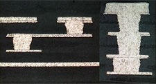
Figure 1: Cross-section of layer 1 to layer 3 staggered copper filled microvia and layer 1 to layer 4 stacked copper filled microvia. Cross-sections were polished and microetched to reveal copper structure.
Figure 1 shows a two-level staggered microvia and a three-level stacked microvia. Both configurations are used in PWBs; however, when both were used on same PWB, the stacked microvia failed during reflow assembly while the staggered microvia did not. The microvias were formed with a UV-CO2 combo laser UV clean followed by desmear, electroless copper, and electrolytic copper fill.
Figure 2: Cross-section of a three-stack microvia failure.
Both stacked and staggered microvias must survive reflow assembly. A cross-section of a failed three-stack microvia shown in Figure 2 revealed a separation between the target pad and plated copper fill at both layers 2 and 4. The microvias were drilled with a UV laser followed by desmear, electroless copper, a copper strike, then copper fill. The UV laser ablation parameter was set to dig into the copper target pad. The UV-drilled microvia failed during reflow assembly.
Figure 3 is SEM photograph of a UV laser-drilled, copper-filled microvia cross-section before assembly reflow. The copper-fill to target pad interface as shown is a complex structure that meanders into the layer 2 plated copper. Arrow (a) points to a UV laser-formed copper burr at the knee of the copper foil. Arrow (b) points to a thin demarcation that follows the copper fill to copper strike interface. Arrow (d) points to the electroless layer between the copper foil and electroplated copper. Arrows (c) and (e) point to interface features that are darker and coarser than the plated copper. The electroplated copper strike to electroless copper to target pad interfaces were obscured by the features created by the UV laser ablation.
Figure 3: UV-only laser-drilled copper-filled microvia: (a) UV-laser-induced burr formed on copper foil; (b) Demarcation between copper fill and copper strike; (c) Feature with different texture compared to the plated copper; (d) Electroless copper layer between copper foil and electroplated copper; (e) Feature with texture different compared to the plated copper.
UV laser-drilled stacked microvias failed reflow assembly more frequently compared to microvias drilled by other laser types. The difference was related to the UV laser created features present between the copper fill and target pad as shown in Figure 3. The features, only observed in UV laser-drilled microvias formed as copper melted and recast in the presence of air, coincide with the weak points that fracture when thermally stressed during reflow assembly. The rest of this article presents SEM photographs of microvias after laser drill and after electroless copper to show the condition of the copper surface of the target pad produced by the commonly practiced laser processes.
Results and Discussion
The PWB manufacturing base uses different laser types, plating chemistries, and laminate materials in the manufacture of PWBs with microvias. A reliable stacked microvia depends on the condition of the target pad after the laser process. Laser drilling is the accepted method of forming microvias. UV Nd:YAG and CO2 lasers were developed to drill microvias and are commercially available in four different configurations to the PWB industry.
1. UV Nd:YAG Laser
The UV laser can micro-machine a variety of materials, including copper and glass-reinforced dielectric laminate to produce unique features. The ability to ablate copper can potentially damage copper surfaces, such as the target pad of a microvia. SEM photographs of target pads touched by the UV beam show evidence of melted copper and copper particles that were explosively ejected from the melted copper surface. Copper flow patterns were visible on the target pad along with porosity and inclusions that were characteristic of the sputtering and recasting of molten copper. Molten copper flow patterns were visible over the surface of the target pad and the rim of the outer layer copper foil surrounding the microvia opening—basically any copper surface the UV beam contacted. Constructions require surface copper thickness thinner than target copper thickness to prevent the UV beam from piercing the target pad copper. In most constructions, UV copper ablation requires entry copper to be less than 0.5-oz. copper weight.
To read the full article, which appeared in the July 2019 issue of PCB007 Magazine, click here.
Share on:


Testimonial
"Advertising in PCB007 Magazine has been a great way to showcase our bare board testers to the right audience. The I-Connect007 team makes the process smooth and professional. We’re proud to be featured in such a trusted publication."
Klaus Koziol - atgSuggested Items
Episode 6 of Ultra HDI Podcast Series Explores Copper-filled Microvias in Advanced PCB Design and Fabrication
10/15/2025 | I-Connect007I-Connect007 has released Episode 6 of its acclaimed On the Line with... American Standard Circuits: Ultra High Density Interconnect (UHDI) podcast series. In this episode, “Copper Filling of Vias,” host Nolan Johnson once again welcomes John Johnson, Director of Quality and Advanced Technology at American Standard Circuits, for a deep dive into the pros and cons of copper plating microvias—from both the fabricator’s and designer’s perspectives.
Nolan’s Notes: Tariffs, Technologies, and Optimization
10/01/2025 | Nolan Johnson -- Column: Nolan's NotesLast month, SMT007 Magazine spotlighted India, and boy, did we pick a good time to do so. Tariff and trade news involving India was breaking like a storm surge. The U.S. tariffs shifted India from one of the most favorable trade agreements to the least favorable. Electronics continue to be exempt for the time being, but lest you think that we’re free and clear because we manufacture electronics, steel and aluminum are specifically called out at the 50% tariff levels.
MacDermid Alpha & Graphic PLC Lead UK’s First Horizontal Electroless Copper Installation
09/30/2025 | MacDermid Alpha & Graphic PLCMacDermid Alpha Electronics Solutions, a leading supplier of integrated materials and chemistries to the electronics industry, is proud to support Graphic PLC, a Somacis company, with the installation of the first horizontal electroless copper metallization process in the UK.
Electrodeposited Copper Foils Market to Grow by $11.7 Billion Over 2025-2032
09/18/2025 | Globe NewswireThe global electrodeposited copper foils market is poised for dynamic growth, driven by the rising adoption in advanced electronics and renewable energy storage solutions.
MacDermid Alpha Showcases Advanced Interconnect Solutions at PCIM Asia 2025
09/18/2025 | MacDermid Alpha Electronics SolutionsMacDermid Alpha Electronic Solutions, a global leader in materials for power electronics and semiconductor assembly, will showcase its latest interconnect innovations in electronic interconnect materials at PCIM Asia 2025, held from September 24 to 26 at the Shanghai New International Expo Centre, Booth N5-E30