


 The Chemical Connection: Reducing Etch System Water Usage, Part 2
 It’s Only Common Sense: Nice Guys Really Can Finish First
 The Right Approach: I Hear the Train A Comin'
A Modified Device Fabrication Process Achieves Enhanced Spin Transport in Graphene
August 5, 2019 | ICN2Estimated reading time: 2 minutes
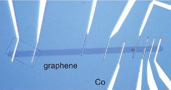
Researchers from the ICN2 Physics and Engineering of Nanodevices Group have proposed a modified graphene-based nanodevice fabrication technique that has increased up to three times the spin lifetime and relaxation length compared to previous work of the same kind. The work was fruit of the collaboration with Imec and K.U. Leuven (Belgium). The results have been published in 2D Materials and are expected to empower investigations on large-scale spintronic applications.
Spintronics is a field of research that was born in the 1980s. It amplifies the potential of traditional electronics by exploiting the electron’s spin degree of freedom, in addition to the usual state of charge. In the end, the goal is the same: to obtain devices to store, process and read information, but with enhanced characteristics such as lower power consumption, less heat dissipation, higher speed, etc. Although spintronics has not yet become as widespread as its conventional predecessor, some current devices are based on this new approach, such as magnetic hard disks, magnetic random access memories and magnetic sensors with varied applications in industrial environments, robotics and automotive industry.
Graphene is a promising material in this field. Spins can flow efficiently in it over long distances, meaning that they do not change their state (let’s say, from “up” to “down”) for a relatively long time. Due to its large-scale production, CVD graphene is becoming popular to fabricate spintronic devices. However, impurities arising from the graphene growth and device fabrication process limit its performance.
A team of scientists from the ICN2 Physics and Engineering of Nanodevices Group, led by ICREA Prof. Sergio O. Valenzuela, has proposed a high-yield device fabrication process from CVD graphene that has improved substantially its spin parameters. The work, whose first author is Zewdu M. Gebeyehu, was fruit of a collaboration with Imec and K.U. Leuven (Belgium). The results have been published in 2D Materials.
They demonstrate a spin signal measured across a 30 µm long channel with room-temperature spin lifetimes of up to 3 ns and spin relaxation lengths of up to 9 µm in monolayer graphene on SiO2/Si substrates. These spin parameters are the highest values for any form of graphene (both exfoliated and CVD graphene) on a standard SiO2/Si substrate.
To achieve this enhanced spin performance, the researchers used CVD graphene grown on a platinum foil and they modified the device fabrication technique so as to reduce the impurity levels associated with the graphene growth and fabrication steps. The latter requires the optimization of several standard processes, involving the preselection of high-quality uniform graphene with low level of impurities, an etching step combining e-beam lithography and oxygen plasma and a suitable post-annealing in high vacuum. The approach can be scaled and allows a highly reproducible fabrication of devices, which is the main requirement for potential industrialization.
The improvement on the spin parameters together with the reproducibility of the device fabrication process brings us closer to the realization of complex circuit architectures for spintronic devices such as spin logic and logic-in-memory for beyond CMOS computing.
Share on:


Suggested Items
Argonne, Toyota Collaborate on Cutting-Edge Battery Recycling Process
05/01/2024 | BUSINESS WIREThe U.S. Department of Energy’s (DOE) Argonne National Laboratory has recently launched a collaboration with Toyota Motor North America that could reduce the nation’s reliance on foreign sources of battery materials.
Real Time with… IPC APEX EXPO 2024: Outlining Rehm's Innovations and Global Presence
05/01/2024 | Real Time with...IPC APEX EXPOMichael Hanke, the chief sales officer for Rehm Thermal Systems, shares insights on the North American market, new machinery, and software development. He also discusses Rehm's turnkey solutions, process flexibility, global presence, and the dedicated team of 700 employees working on global solutions.
The Knowledge Base: A CM’s Perspective on Box Build Practices
04/30/2024 | Mike Konrad -- Column: The Knowledge BaseIn the ever-evolving landscape of electronics manufacturing, the box-build process stands out as a critical phase that bridges the gap between individual component manufacturing and the delivery of a fully functional electronic system. This intricate procedure, encompassing the assembly of everything from PCBs to wire harnesses and mechanical enclosures, demands a high level of precision, efficiency, and innovation. As the electronics assembly industry expands and diversifies, understanding the best practices within box-build assembly has become paramount for manufacturers aiming to stay ahead in a competitive market.
TSMC Certifies Ansys Multiphysics Platforms, Enabling Next-Gen AI and HPC Chips
04/30/2024 | PRNewswireAnsys announced the certification of its power integrity platforms for TSMC's N2 technology full production release. Both Ansys RedHawk-SC and Ansys Totem are certified for power integrity signoff on the N2 process, delivering significant speed and power advantages for high performance computing, mobile chips, and 3D-IC designs.
Koh Young Showcases Award-winning Inspection Solutions at SMTconnect with SmartRep in Hall 4A.225
04/25/2024 | Koh Young TechnologyKoh Young Technology, the industry leader in True 3D measurement-based inspection solutions, will showcase an array of award-winning inspection and measurement solutions at SMTconnect alongside its sales partner, SmartRep, in booth 4A.225 at NürnbergMesse from June 11-13, 2023. The following offers a glimpse into what Koh Young will present at the tradeshow: