


 Dan’s Biz Bookshelf: ‘The Next RenAIssance: AI and the Expansion of Human Potential’
 The Chemical Connection: When the Industry Moves Faster Than the Standards
 Driving Innovation: Selecting the Right Laser Source


Innovative Electroplating Processes for IC Substrates
August 27, 2019 | S. Dharmarathna, S. Maddux, C. Benjamin, I. Li, W. Bowerman, K. Feng, and J. Watkowski, MacDermid Alpha Electronics SolutionsEstimated reading time: 3 minutes
Abstract
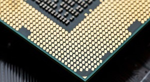
In this era of electronics miniaturization, high-yield and low-cost integrated circuit (IC) substrates play a crucial role by providing a reliable method of high-density interconnection (HDI) of the chip to the board. To maximize substrate real estate, the distance between copper traces—also known as line and space (L/S)- should be minimized. Typical PCB technology consists of L/S larger than 40 µm whereas more advanced wafer-level technology currently sits at or around 2 µm L/S. In the past decade, the chip size has decreased significantly along with the L/S on the substrate. The decreasing chip scales and smaller L/S distances have created unique challenges for both the printed circuit board (PCB) industry and the semiconductor industry.
Fan-out panel-level packaging (FOPLP) is a new manufacturing technology that seeks to bring the PCB world and IC/semiconductor world even closer. While FOPLP is still an emerging technology, the amount of high-volume production in this market space provide a financial incentive to develop innovative solutions to enable its ramp-up. The most important performance aspect of the fine-line plating in this market space is plating uniformity or planarity. Plating uniformity, trace/via top planarity (which measures how flat the top of the traces), and vias are a few major features. This is especially important in multilayer processing, as nonuniformity on a lower layer can be transferred to successive layers, disrupting the device design with catastrophic consequences, such as short circuits. Additionally, a non-planar surface could also result in signal transmission loss by distortion of the connecting points (i.e., vias and traces). Therefore, plating solutions that provide a uniform, planar profile without any special post-treatment are quite desirable.
Here, we discuss innovative additive packages for direct-current copper electroplating specifically for IC substrates with capabilities such as embedded trench fill and simultaneous through-hole plating and via filling with an enhanced pattern plate. These new solutions not only offer better trace profile, but they also deliver via fill and through-hole plating. We also describe two electrolytic copper plating processes, the selection of which could be based on the via size and the dimple requirements of the application. Process I offers great via fill for deeper vias up to 80–120 µm diameter and 50–100µm deep. Process II is more suitable for shallow smaller vias 50–75 µm diameter and 30–50 µm deep.
In this article, we show that these two processes provide excellent surface uniformity and trace profile while also providing via filling and through-hole plating capabilities when controlled within given parameters. Process optimization and thermal and physical characterization of the metallization are also presented.
Introduction
The IC substrate is the highest level of miniaturization in PCB technology, providing the connection between the IC chip and the PCB. These connections are created through a network of electrically conductive copper traces and through-holes. The density of the traces is a crucial factor in terms of miniaturization, speed, and portability of consumer electronics. Trace density has grown immensely over the past few decades to meet today’s printed circuit designs, which include thin core material, fine-line widths, and smaller diameter through-holes and blind vias. The development of fan-out panel-level packaging (FOPLP) has been a topic among the microelectronics community for some time.
The main driving forces to push this new technology are cost and productivity. Traditional fan-out wafer-level packaging (FOWLP) uses a 300-mm wafer as the production vehicle because larger wafers are difficult to obtain. Therefore, the FOWLP has a limitation on the basic unit of process, thereby increasing the processing steps, manpower, and cost while also having a low yield. The advantage of using a PCB-like substrate is that manufacturers have more design flexibility and surface area compared to the wafer. As an example, a 610 x 457 mm panel has almost four times the surface area of a 300-mm wafer. Therefore, processing a panel this size drastically reduces cost, time, and processing steps. This is a huge advantage for the high-volume production market.
To read the full article, which appeared in the August 2019 issue of PCB007 Magazine, click here.
Share on:


Testimonial
"The I-Connect007 team is outstanding—kind, responsive, and a true marketing partner. Their design team created fresh, eye-catching ads, and their editorial support polished our content to let our brand shine. Thank you all! "
Sweeney Ng - CEE PCBSuggested Items
Driving Innovation: Selecting the Right Laser Source
04/28/2026 | Simon Khesin -- Column: Driving InnovationWhen I first joined Schmoll Maschinen, I brought experience from almost every PCB process, except for laser. As I immersed myself in laser processing, I realized why it can seem so daunting to a newcomer. The complexity arises from three intersecting factors: A vast variety of laser sources: CO2, UV-nano, green-pico, UV-pico, IR-pico, and others; a diverse range of applications: Drilling, cutting, ablation, and more; and an extensive list of materials: These have vastly different absorption rates. Choosing the right machine or laser source is rarely trivial. Even for experienced engineers, answering "Which source is best?" requires examining the business's specific goals.
Institute of Circuit Technology Spring Seminar 2026: A Bright Future in Europe
04/23/2026 | Pete Starkey, I-Connect007Through the leafy lanes and spring flowers of Warwickshire and back to Meridan, the traditional centre of England, and now officially part of the Metropolitan Borough of Solihull in the county of the West Midlands, I attended the Annual General Meeting and Spring Seminar of the Institute of Circuit Technology (ICT) on April 14. Out of the AGM came notable changes in leadership at the top of the Institute: the retirement of Mat Beadel as chair and Emma Hudson as technical director. Effective May 1, Steve Driver is the new chair, and Alun Morgan is the new technical director.
ACCM Unveils Negative and Near-zero CTE Materials for Large-Format AI Chips
04/21/2026 | Advanced Chip and Circuit MaterialsAdvanced Chip and Circuit Materials, Inc. (ACCM) has launched two new materials: Celeritas HM50, with a negative coefficient of thermal expansion (CTE) of -8 ppm/°C to offset the positive CTE and expansion of copper with temperature on circuit boards, and Celeritas HM001, with near-zero CTE and the low-loss performance needed for high-speed signal layers to 224 Gb/s and faster in artificial intelligence (AI) circuits.
Fresh PCB Concepts: Designing PCBs for Harsh Environments—Reliability Is Engineered Upstream
04/23/2026 | Team NCAB -- Column: Fresh PCB ConceptsWhen engineers hear the phrase “harsh environment,” they usually think of the extreme temperature swings, vibration and shock, pressure changes, or radiation in aerospace. However, aerospace is not the only harsh environment where electronic assemblies must survive. Automotive power electronics, downhole oil and gas tools, marine controls, rail systems, defense platforms, and industrial automation equipment all expose PCBs to environments that are equally unforgiving. The stress mechanisms may differ, but the physics does not.
Advanced Packaging for AI: Reliability Starts at the Cu/Cu/Cu Microvia Junction
04/20/2026 | Kuldip Johal, MKS' AtotechThe rapid growth of AI computing, from training clusters to inference at scale, is reshaping demand across the entire electronics supply chain. Advances in technology requirements, such as higher bandwidth, lower latency, and greater compute density, are driving the development of advanced packaging technologies and transforming the PCB industry across design, manufacturing, testing, and even architecture.