


 The Right Approach: I Hear the Train A Comin'
 It’s Only Common Sense: OCCAM—the Time Is Now
 Marcy's Musings: The Growing Industry
Light and Sound in Silicon Chips: The Slower the Better
September 17, 2019 | BAR-ILAN UNIVERSITYEstimated reading time: 3 minutes
Integrated circuits in silicon enable our digital era. The capabilities of electronic circuits have been extended even further with the introduction of photonics: components for the generation, guiding and detection of light. Together, electronics and photonics support entire systems for data communication and processing, all on a chip. However, there are certain things that even electrical and optical signals can't do simply because they move too fast.
Sometimes moving slowly is actually better, according to Prof. Avi Zadok of Bar-Ilan University's Faculty of Engineering and Institute of Nanotechnology and Advanced Materials. "Important signal processing tasks, such as the precise selection of frequency channels, require that data is delayed over time scales of tens of nano-seconds. Given the fast speed of light, optical waves propagate over many meters within these timeframes. One cannot accommodate such path lengths in a silicon chip. It is unrealistic. In this race, fast doesn't necessarily win."
The problem, in fact, is a rather old one. Analog electronic circuits have been facing similar challenges in signal processing for sixty years. An excellent solution was found in the form of acoustics: A signal of interest is converted from the electrical domain to the form of an acoustic wave. The speed of sound, of course, is slower than that of light by a factor of 100,000. Acoustic waves acquire the necessary delays over tens of micro-meters instead of meters. Such path lengths are easily accommodated on-chip. Following propagation, the delayed signal can be converted back to electronics.
In a new work published in the journal Nature Communications, Zadok and co-workers carry over this principle to silicon-photonic circuits. "There are several difficulties with introducing acoustic waves to silicon chips," says doctoral student Dvir Munk, of Bar-Ilan University, who participated in the study. "The standard layer structure used for silicon photonics is called silicon on insulator. While this structure guides light very effectively, it cannot confine and guide sound waves. Instead, acoustic waves just leak away." Due to this difficulty, previous works that combine light and sound waves in silicon do not involve the standard layer structure. Alternatively, hybrid integration of additional, nonstandard materials was necessary.
"That first challenge can be overcome by using acoustic waves that propagate at the upper surface of the silicon chip," continues Munk. "These surface acoustic waves do not leak down as quickly. Here, however, there is another issue: Generation of acoustic waves usually relies on piezo-electric crystals. These crystals expand when a voltage is applied to them. Unfortunately, this physical effect does not exist in silicon, and we much prefer to avoid introducing additional materials to the device."
As an alternative, students Munk, Moshe Katzman and coworkers relied on the illumination of metals. "Incoming light carries the signal of interest," explains Katzman. "It irradiates a metal pattern on the chip. The metals expand and contract, and strain the silicon surface below. With proper design, that initial strain can drive surface acoustic waves. In turn, the acoustic waves pass across standard optical waveguides in the same chip. Light in those waveguides is affected by the surface waves. In this way, the signal of interest is converted from one optical wave to another via acoustics. In the meantime, significant delay is accumulated within very short reach."
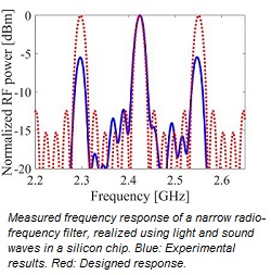
The concept combines light and sound in standard silicon with no suspension of membranes or use of piezo-electric crystals. Acoustic frequencies up to 8 GHz are reached, however the concept is scalable to 100 GHz. The working principle is applicable to any substrate, not only silicon. Applications are presented as well: the concept is used in narrowband filters of input radio-frequency signals. The highly selective filters make use of 40 nano-second long delays. "Rather than use five meters of waveguide, we achieve this delay within 150 microns," says Munk.
Prof. Zadok summarizes: "Acoustics is a missing dimension in silicon chips because acoustics can complete specific tasks that are difficult to do with electronics and optics alone. For the first time we have added this dimension to the standard silicon photonics platform. The concept combines the communication and bandwidth offered by light with the selective processing of sound waves."
One potential application of such devices is in future cellular networks, widely known as 5G. Digital electronics alone might not be enough to support the signal processing requirements in such networks. Light and sound devices might do the trick.
Share on:


Suggested Items
Real Time with… IPC APEX EXPO 2024: Exploring the Future of Surface Finishes
04/25/2024 | Real Time with...IPC APEX EXPOJoe McGurran, product marketing director for MKS Atotech, looks into the future of surface finishes, discussing less nickel, reduced thickness, technologies influencing HDI and UHDI, and the benefits of nickel-free surface finishes. He also touches on popular finishes like ENIG and palladium immersion gold and discusses the value proposition of making a change.
Designer’s Notebook: What Designers Need to Know About Manufacturing, Part 2
04/24/2024 | Vern Solberg -- Column: Designer's NotebookThe printed circuit board (PCB) is the primary base element for providing the interconnect platform for mounting and electrically joining electronic components. When assessing PCB design complexity, first consider the component area and board area ratio. If the surface area for the component interface is restricted, it may justify adopting multilayer or multilayer sequential buildup (SBU) PCB fabrication to enable a more efficient sub-surface circuit interconnect.
IDTechEx Report Unveils 3D Electronics Status and Opportunities
04/22/2024 | PRNewswire3D electronics is an emerging manufacturing approach that enables electronics to be integrated within or onto the surface of objects. 3D electronic manufacturing techniques empower new features, including mass customizability, greater integration, and improved sustainability in the electronics industry.
NASA, Japan Advance Space Cooperation, Sign Agreement for Lunar Rover
04/11/2024 | NASANASA Administrator Bill Nelson and Japan’s Minister of Education, Culture, Sports, Science and Technology (MEXT) Masahito Moriyama have signed an agreement to advance sustainable human exploration of the Moon.
Lockheed Martin Conducts Historic LRASM Flight Test
04/04/2024 | Lockheed MartinThe U.S. Navy in partnership with Lockheed Martin [NYSE: LMT] successfully conducted a historic Long-Range Anti-Ship Missile (LRASM) flight test with four missiles simultaneously in flight.