


 The Right Approach: I Hear the Train A Comin'
 It’s Only Common Sense: OCCAM—the Time Is Now
 Marcy's Musings: The Growing Industry
Tiny Intel EMIB Helps Chips ‘Talk’ with Each Other
November 27, 2019 | IntelEstimated reading time: 1 minute
Most chips in today’s smartphones, computers and servers are comprised of multiple smaller chips invisibly sealed inside one rectangular package.
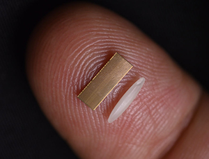
How do these multiple chips — often including CPU, graphics, memory, IO and more — communicate? An Intel innovation called EMIB (embedded multi-die interconnect bridge) is a complex multi-layered sliver of silicon no bigger than a grain of rice. It lets chips fling enormous quantities of data back and forth among adjoining chips at blinding speeds: several gigabytes per second.
Today, Intel EMIBs speed the flow of data inside nearly 1 million laptops and field programmable gate array devices worldwide. That number will soon soar and include more products as EMIB technology enters the mainstream. For example, Intel’s Ponte Vecchio processor, a general-purpose GPU the company unveiled Nov. 17, contains EMIB silicon.
To meet customers’ unique needs, this innovative technology allows chip architects to cobble together specialized chips faster than ever. And compared with an older, competing design called an interposer — in which chips inside a package sit atop what is essentially a single electronic baseboard, with each chip plugged into it — tiny, flexible, cost-effective EMIB silicon offers an 85% increase in bandwidth. That can make your tech — laptop, server, 5G processor, graphics card— run dramatically faster. And next-generation EMIB could double or even triple that bandwidth.
Intel’s embedded multi-die interconnect bridge (EMIB) technology helps multiple chips – CPU, graphics, memory, IO and more — communicate. EMIB is a complex multi-layered sliver of silicon no bigger than a grain of Basmati rice that moves large quantities of data among adjoining chips.
Share on:


Suggested Items
Warm Windows and Streamlined Skin Patches – IDTechEx Explores Flexible and Printed Electronics
04/26/2024 | IDTechExFlexible and printed electronics can be integrated into cars and homes to create modern aesthetics that are beneficial and easy to use. From luminous car controls to food labels that communicate the quality of food, the uses of this technology are endless and can upgrade many areas of everyday life.
iNEMI Packaging Tech Topic Series: Role of EDA in Advanced Semiconductor Packaging
04/26/2024 | iNEMIAdvanced semiconductor packaging with heterogenous integration has made on-package integration of multiple chips a crucial part of finding alternatives to transistor scaling. Historically, EDA tools for front-end and back-end design have evolved separately; however, design complexity and the increased number of die-to-die or die-to-substrate interconnections has led to the need for EDA tools that can support integration of overall design planning, implementation, and system analysis in a single cockpit.
Koh Young Showcases Award-winning Inspection Solutions at SMTconnect with SmartRep in Hall 4A.225
04/25/2024 | Koh Young TechnologyKoh Young Technology, the industry leader in True 3D measurement-based inspection solutions, will showcase an array of award-winning inspection and measurement solutions at SMTconnect alongside its sales partner, SmartRep, in booth 4A.225 at NürnbergMesse from June 11-13, 2023. The following offers a glimpse into what Koh Young will present at the tradeshow:
Real Time with… IPC APEX EXPO 2024: Plasmatreat: Innovative Surface Preparation Solutions
04/25/2024 | Real Time with...IPC APEX EXPOIn this interview, Editor Nolan Johnson speaks with Hardev Grewal, CEO and president of Plasmatreat, a developer of atmospheric plasma solutions. Plasmatreat uses clean compressed air and electricity to create plasma, offering environmentally friendly methods for surface preparation. Their technology measures plasma density for process optimization and can remove organic micro-contamination. Nolan and Hardev also discuss REDOX-Tool, a new technology for removing metal oxides.
Nanotechnology Market to Surpass $53.51 Billion by 2031
04/25/2024 | PRNewswireSkyQuest projects that the nanotechnology market will attain a value of USD 53.51 billion by 2031, with a CAGR of 36.4% over the forecast period (2024-2031).