


 The Chemical Connection: Reducing Etch System Water Usage, Part 2
 It’s Only Common Sense: Nice Guys Really Can Finish First
 The Right Approach: I Hear the Train A Comin'
Quik-Pak Announces Substrate Development Service
February 11, 2020 | Quik-PakEstimated reading time: 1 minute
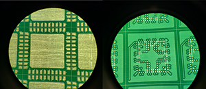
Quik-Pak, a provider of innovative microelectronic packaging and assembly solutions, today announced its substrate design, fabrication and assembly service. Utilizing virtually any substrate type, Quik-Pak can create turnkey solutions for substrate-based assemblies to accommodate customers’ unique packaging requirements, with delivery times at least 50% faster than those of competitive services.
Quik-Pak’s substrate service targets both ICs and MEMS, and its ability to accommodate all types of substrates provides engineering flexibility that allows greater design freedom for a wide range of advanced packages. Quik-Pak has offered this capability, in a limited fashion, for several years. Its success has spurred the company to step up activity—particularly in the face of broadening demand for custom packaging solutions that can fill the gaps not met by standard, off-the-shelf packages.
One key driver for this demand is the increased need for custom RF packages in the face of 5G’s imminent rollout. Technologies in which Quik-Pak specializes, such as laminate quad flat no-lead (QFN) and organic QFN for flip-chips, are well suited to integration and customization. The service can also accommodate 3D packaging, ball grid arrays (BGAs), systems-in-package (SiPs) and multichip modules (MCMs).
According to Quik-Pak Chief Operating Officer Ken Molitor, “We can tune our process to optimize the customer’s desired parameter—size, performance, application—creating a solution in about five weeks, from initial consultation to finished assembly. Other services can take five weeks to complete the design alone and up to 16 weeks to deliver the assembled package. With this combination of quality and speed, Quik-Pak is poised to broaden the reach of our service to address new markets and applications, such as military, medical, sensors and other custom arenas.”
Quik-Pak will be showcasing its full range of capabilities, including its new substrate service offering, in the expo hall at the 16th annual IMAPS International Conference on Device Packaging. The company is also a sponsor of the event, to be held March 2-5, 2020, in Fountain Hills, Ariz.
Share on:


Suggested Items
Real Time with… IPC APEX EXPO 2024: My Role as a Technology Solutions Director
05/02/2024 | Real Time with...IPC APEX EXPOPeter Tranitz, senior director of technology solutions at IPC, shares insights into his role as the design initiative lead. He details his advocacy work, industry support, and the responsibilities of the design initiative committee. The conversation also covers the revamping of standards, the IPC Design Competition, and the implementation of design rules in software tools.
Real Time with… IPC APEX EXPO 2024: Ventec Discusses New Pro-bond Family of Advanced Products
05/01/2024 | Real Time with...IPC APEX EXPOChris Hanson, Ventec's Global Head of IMS Technology, outlines the launch of four pro-bond formulas that deliver an outstanding combination of low dissipation factor (Df) with a dielectric constant (Dk) range to maximize the design window for critical PCB parameters. As Chris points out, Pro-bond is designed for low-loss, high-speed applications, while thermal-bond dissipates heat from a component through the board to a heat sink.
IPC's Vision for Empowering PCB Design Engineers
04/30/2024 | Robert Erickson, IPCAs architects of innovation, printed circuit board designers are tasked with translating increasingly complex concepts into tangible designs that power our modern world. IPC provides the necessary community, standards framework, and education to prepare these pioneers as they explore the boundaries of what’s possible, equipping engineers with the knowledge, skills, and resources required to thrive in an increasingly dynamic field.
On the Line With… Talks With Cadence Expert on SI/PI for PCB Designers
05/02/2024 | I-Connect007In “PCB 3.0: A New Design Methodology—SI/PI for PCB Designers,” subject matter expert Brad Griffin, Cadence Design Systems, discusses how an intelligent system design methodology can move some signal and power integrity decision-making into the physical design space, offering real-time feedback.
iNEMI Packaging Tech Topic Series: Role of EDA in Advanced Semiconductor Packaging
04/26/2024 | iNEMIAdvanced semiconductor packaging with heterogenous integration has made on-package integration of multiple chips a crucial part of finding alternatives to transistor scaling. Historically, EDA tools for front-end and back-end design have evolved separately; however, design complexity and the increased number of die-to-die or die-to-substrate interconnections has led to the need for EDA tools that can support integration of overall design planning, implementation, and system analysis in a single cockpit.