


 The Chemical Connection: Reducing Etch System Water Usage, Part 2
 It’s Only Common Sense: Nice Guys Really Can Finish First
 The Right Approach: I Hear the Train A Comin'
STMicroelectronics Introduces Standalone VBUS-Powered Controller for 5V USB-C Charging Applications
March 20, 2020 | STMicroelectronicsEstimated reading time: 1 minute
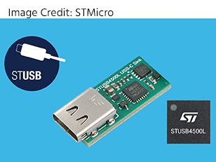
The STUSB4500L from STMicroelectronics is a small-footprint addition to the Company’s USB-C controller IC family designed and certified for pure 5V sink-only applications. All mandatory features to use the USB-C connector as a 5V universal power plug are integrated, allowing designers to implement USB-C charging solutions quickly and easily without studying the standard or writing code.
USB-C is rapidly becoming established as a replacement for Micro-B or Mini-B plugs, for both power and data connections, as it offers the advantages of reversible orientation and greater robustness — up to 10,000 connect/disconnect cycles.
ST’s new USB-C controller IC is a stand-alone, plug-and-play interface product, targeting low-voltage applications such as Bluetooth speakers, computer accessories, Wi-Fi access points, point-of-sale equipment, LED lighting, and USB dongles. It can also be used for powering equipment such as single-board computers and hardware development kits. The controller IC runs without additional code and requires no external support from the microcontroller, which eases adoption of the USB-C connector standard by saving time-consuming design work.
The STUSB4500L is auto-powered via VBUS from the connected source and does not need to be supplied from a local battery or on-board power. Zero leakage current prevents draining the battery when not charging. Input over-voltage protection prevents low-voltage equipment being damaged if it is incorrectly connected, for example, to a 20V source from a USB PD AC adapter rather than the required 5V supply.
Further features include ‘dead-battery’ support to ensure correct identification by the source when the battery is fully discharged, true cold-socket implementation which keeps the VBUS switch open by default until safe 5V input power is supplied, source power-budget identification and error-recovery support to ensure correct re-starting when a fault is triggered.
The STUSB4500L is in production now, in a choice of 4mm x 4mm QFN-24 package or 2.6mm x 2.6mm CSP-25 chip-scale package, priced from $0.70 and $0.75 respectively for orders of 1000 pieces.
To ease prototyping, the reference design EVAL-SCS002V1, which has a small footprint of just 2.5 cm², can be ordered from ST or distributors. For fast implementation into proprietary designs, the full PCB design libraries can be downloaded free of charge from st.com.
Share on:


Suggested Items
Real Time with… IPC APEX EXPO 2024: My Role as a Technology Solutions Director
05/02/2024 | Real Time with...IPC APEX EXPOPeter Tranitz, senior director of technology solutions at IPC, shares insights into his role as the design initiative lead. He details his advocacy work, industry support, and the responsibilities of the design initiative committee. The conversation also covers the revamping of standards, the IPC Design Competition, and the implementation of design rules in software tools.
Real Time with… IPC APEX EXPO 2024: Ventec Discusses New Pro-bond Family of Advanced Products
05/01/2024 | Real Time with...IPC APEX EXPOChris Hanson, Ventec's Global Head of IMS Technology, outlines the launch of four pro-bond formulas that deliver an outstanding combination of low dissipation factor (Df) with a dielectric constant (Dk) range to maximize the design window for critical PCB parameters. As Chris points out, Pro-bond is designed for low-loss, high-speed applications, while thermal-bond dissipates heat from a component through the board to a heat sink.
IPC's Vision for Empowering PCB Design Engineers
04/30/2024 | Robert Erickson, IPCAs architects of innovation, printed circuit board designers are tasked with translating increasingly complex concepts into tangible designs that power our modern world. IPC provides the necessary community, standards framework, and education to prepare these pioneers as they explore the boundaries of what’s possible, equipping engineers with the knowledge, skills, and resources required to thrive in an increasingly dynamic field.
On the Line With… Talks With Cadence Expert on SI/PI for PCB Designers
05/02/2024 | I-Connect007In “PCB 3.0: A New Design Methodology—SI/PI for PCB Designers,” subject matter expert Brad Griffin, Cadence Design Systems, discusses how an intelligent system design methodology can move some signal and power integrity decision-making into the physical design space, offering real-time feedback.
iNEMI Packaging Tech Topic Series: Role of EDA in Advanced Semiconductor Packaging
04/26/2024 | iNEMIAdvanced semiconductor packaging with heterogenous integration has made on-package integration of multiple chips a crucial part of finding alternatives to transistor scaling. Historically, EDA tools for front-end and back-end design have evolved separately; however, design complexity and the increased number of die-to-die or die-to-substrate interconnections has led to the need for EDA tools that can support integration of overall design planning, implementation, and system analysis in a single cockpit.