


 Flexible Thinking: Designing Flex Circuits for Dynamic Reliability
 Global PCB Connections: Rigid-flex and Flexible PCBs—The Backbone of Modern Electronics
 Happy’s Tech Talk #29: Bend-to-Install Semi-flex FR-4


ESA Approval for Ventec VT-901 Material in ACB Belgium Rigid & Flex-Rigid Production
May 26, 2020 | Ventec International Group Co., Ltd.Estimated reading time: 2 minutes
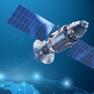
Ventec International Group Co., Ltd. is pleased to announce that its VT-901 polyimide material is now fully qualified by ESA in ACB Belgium’s manufacturing process for rigid and rigid-flex polyimide PCBs and HDI PCBs.
With high Td (395oC), a Tg of 250oC and Low-Axis CTE (50), Ventec's VT-901 polyimide material provides the extremely high reliability performance demanded by ACB’s flex & flex-rigid and HDI PCB manufacturing process that meets ESA requirements.
Ventec manufactures all VT-901 polyimide using specially designed treaters with multiple stage filtration systems and 100% Automated Optical Inspection (AOI) for prepreg FOD-control. The same specialist equipment is used for the production of thin-core laminates for use in the most demanding space and aerospace PCB applications. ACB's state-of-the-art PCB manufacturing facility in Dendermonde (Belgium) and the AS9100 Rev D accreditation of Ventec's manufacturing and distribution facilities, position both companies as market-leaders within the space and aerospace electronics supply chain.
Joachim Verhegge, ACB’s Product Engineering Manager, says: 'Meeting and exceeding the highest possible standards of quality and performance is our highest priority. We are pleased to receive ESA approval for the use of Ventec's material in our designs and look forward to continuing to work closely with ESA in meeting their requirements.'
Mark Goodwin, Ventec COO EMEA & USA, commented: ‘I'm delighted with our long-term technology partnership with ACB, assisting them through close cooperation to further strengthen their position for aerospace-standard solutions and finished PCBs. The ESA approval demonstrates the thermal robustness of Ventec VT-901 polyimide and its suitability for use in high reliability rigid and flex rigid multi-layers in the demanding aerospace sector.'
Ventec International is a world leader in the production of polyimide & high reliability epoxy laminates and prepregs and specialist provider of thermal management and IMS solutions. Further information about Ventec’s solutions and the company’s wide variety of products is available at www.venteclaminates.com and/or by downloading the Ventec APP.
About Ventec International Group
Ventec International is a premier supplier to the Global PCB industry. With volume manufacturing facilities in Taiwan and China and distribution locations and manufacturing sites in both the US and Europe, Ventec specializes in advanced copper clad glass reinforced and metal backed substrates. Ventec materials, which include high-quality enhanced FR4, high-speed/low-loss- & high-performance IMS material technology and an advanced range of thermal management solutions, are manufactured by Ventec using strict quality-controlled processes that are certified to AS9100 Revision D, IATF 16949:2016 and ISO 9001:2015, and are backed by a fully controlled and managed global supply chain, sales- and technical support-network.
For more information, visit www.venteclaminates.com.
Share on:


Testimonial
"Our marketing partnership with I-Connect007 is already delivering. Just a day after our press release went live, we received a direct inquiry about our updated products!"
Rachael Temple - AlltematedSuggested Items
I-Connect007 Releases The Printed Circuit Designer’s Guide to… Direct Metallization: A Guide to Complex PCB Fabrication
05/13/2026 | I-Connect007As PCB complexity continues to accelerate, fabricators and OEMs are reevaluating long-standing manufacturing processes to meet the demands of AI, HDI, advanced packaging, and next-generation electronics. To address these evolving challenges, I-Connect007 is proud to announce the release of The Printed Circuit Designer’s Guide to… Direct Metallization: A Guide to Complex PCB Fabrication, authored by MacDermid Alpha Solution’s Carmichael Gugliotti.
Driving Innovation: Selecting the Right Laser Source
04/28/2026 | Simon Khesin -- Column: Driving InnovationWhen I first joined Schmoll Maschinen, I brought experience from almost every PCB process, except for laser. As I immersed myself in laser processing, I realized why it can seem so daunting to a newcomer. The complexity arises from three intersecting factors: A vast variety of laser sources: CO2, UV-nano, green-pico, UV-pico, IR-pico, and others; a diverse range of applications: Drilling, cutting, ablation, and more; and an extensive list of materials: These have vastly different absorption rates. Choosing the right machine or laser source is rarely trivial. Even for experienced engineers, answering "Which source is best?" requires examining the business's specific goals.
Institute of Circuit Technology Spring Seminar 2026: A Bright Future in Europe
04/23/2026 | Pete Starkey, I-Connect007Through the leafy lanes and spring flowers of Warwickshire and back to Meridan, the traditional centre of England, and now officially part of the Metropolitan Borough of Solihull in the county of the West Midlands, I attended the Annual General Meeting and Spring Seminar of the Institute of Circuit Technology (ICT) on April 14. Out of the AGM came notable changes in leadership at the top of the Institute: the retirement of Mat Beadel as chair and Emma Hudson as technical director. Effective May 1, Steve Driver is the new chair, and Alun Morgan is the new technical director.
ACCM Unveils Negative and Near-zero CTE Materials for Large-Format AI Chips
04/21/2026 | Advanced Chip and Circuit MaterialsAdvanced Chip and Circuit Materials, Inc. (ACCM) has launched two new materials: Celeritas HM50, with a negative coefficient of thermal expansion (CTE) of -8 ppm/°C to offset the positive CTE and expansion of copper with temperature on circuit boards, and Celeritas HM001, with near-zero CTE and the low-loss performance needed for high-speed signal layers to 224 Gb/s and faster in artificial intelligence (AI) circuits.
Fresh PCB Concepts: Designing PCBs for Harsh Environments—Reliability Is Engineered Upstream
04/23/2026 | Team NCAB -- Column: Fresh PCB ConceptsWhen engineers hear the phrase “harsh environment,” they usually think of the extreme temperature swings, vibration and shock, pressure changes, or radiation in aerospace. However, aerospace is not the only harsh environment where electronic assemblies must survive. Automotive power electronics, downhole oil and gas tools, marine controls, rail systems, defense platforms, and industrial automation equipment all expose PCBs to environments that are equally unforgiving. The stress mechanisms may differ, but the physics does not.