


 The Big Picture: Our Big ‘Why’ in the Age of AI
 The Chemical Connection: Through-glass Vias in Glass Substrates
 It’s Only Common Sense: Why Sales Teams Fail (and How to Fix Them)


MacDermid Alpha Releases Complete Semi-Additive Process for IC Substrates and Panel Level Packaging: Systek SAP
June 4, 2020 | MacDermid Alpha Electronics SolutionsEstimated reading time: 1 minute
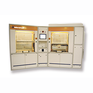
MacDermid Alpha Electronics Solutions, a global leader in specialty materials for electronics, announces the release of Systek SAP.
The MacDermid Alpha Systek SAP is a family of high-performance build-up processes for IC substrate RDL that provide multiple process flows for different materials as well as revolutionary technology innovations in the desmear, conditioning, activation and metallization steps.
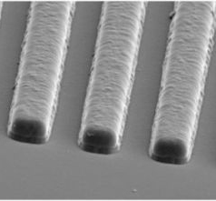
With Systek SAP, new design possibilities in IC substrate manufacturing of high-density circuitry are now available for fine-line, ultra fine-line and flex materials. Systek SAP starts with a four-step desmear process that can be calibrated to optimally prepare multiple substrate materials, imparting minimal roughness while ensuring clean via side walls and copper target pads. The subsequent conditioner process ensures adsorption of the palladium catalyst into the substrate.
The Systek SAP copper metallization process includes an ionic palladium activation system, a zero-stress electroless copper metallization process, and an optional anti-tarnish. Together, the new technologies in the Systek SAP family of semi-additive processes provide substrate manufacturers an easy-to-use toolset for creating RDL with dimensions down to 5/5 micron line/space for very high-density packaging.
“The Systek SAP process represents the pinnacle of years of experience in many aspects of high technology circuit metallization. IC substrate fabricators expanding capacity into new designs are excited about the systems innovations that they can take advantage of in manufacturing reduced roughness, high-density packaging designs for next-gen devices.” said Bill Bowerman, Director of Primary Metallization, Circuitry Solutions.
For more information on Systek SAP, please visit MacDermidAlpha.com
About MacDermid Alpha Electronics Solutions
Through the innovation of specialty chemicals and materials under our Alpha, Compugraphics, Kester, and MacDermid Enthone brands, MacDermid Alpha Electronics Solutions provides solutions that power electronics interconnection. We serve all global regions and every step of device manufacturing within each segment of the electronics supply chain. The experts in our Semiconductor Solutions, Circuitry Solutions, and Assembly Solutions divisions collaborate in design, implementation, and technical service to ensure success for our partner clients. Our solutions enable our customers’ manufacture of extraordinary electronic devices at high productivity and reduced cycle time. Find out more at MacDermidAlpha.com.
Share on:


Suggested Items
North American EMS Industry Shipments Down 9.3% in May
06/25/2025 | Global Electronics AssociationIPC announced the May 2025 findings from its North American Electronics Manufacturing Services (EMS) Statistical Program. The book-to-bill ratio stands at 1.43.
North American PCB Industry Sales Up 21.4% in May
06/25/2025 | Global Electronics AssociationIPC announced the May 2025 findings from its North American Printed Circuit Board (PCB) Statistical Program. The book-to-bill ratio stands at 1.03.
Chiplets and the Like are Redefining Microelectronics
06/25/2025 | productronicaThe performance of modern AI and high-performance computing applications can only be achieved with high-performance semiconductor technology.
United Electronics Corporation Advances Manufacturing Capabilities with Schmoll MDI-ST Imaging Equipment
06/24/2025 | United Electronics CorporationUnited Electronics Corporation has successfully installed the advanced Schmoll MDI-ST (XL) imaging equipment at their advanced printed circuit board facility. This significant technology investment represents a continued commitment to delivering superior products and maintaining their position as an industry leader in precision PCB manufacturing.
STMicroelectronics Introduces Advanced Human Presence Detection Solution to Enhance Laptop and PC User Experience
06/24/2025 | STMicroelectronicsSTMicroelectronics, a global semiconductor leader serving customers across the spectrum of electronics applications, introduces a new Human Presence Detection (HPD) technology for laptops, PCs, monitors and accessories, delivering more than 20% power consumption reduction per day in addition to improved security and privacy.