


 Dan’s Biz Bookshelf: ‘The Next RenAIssance: AI and the Expansion of Human Potential’
 The Chemical Connection: When the Industry Moves Faster Than the Standards
 Driving Innovation: Selecting the Right Laser Source


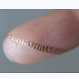
Applied Materials, BE Semiconductor Industries to Accelerate Chip Integration Technology
October 22, 2020 | Globe NewswireEstimated reading time: 2 minutes
Applied Materials, Inc. and BE Semiconductor Industries N.V. announced an agreement to develop the industry’s first complete and proven equipment solution for die-based hybrid bonding, an emerging chip-to-chip interconnect technology that enables heterogeneous chip and subsystem designs for applications including high-performance computing, AI and 5G.
As traditional 2D scaling slows, the semiconductor industry is shifting towards heterogeneous design and chip integration as a new way to deliver improvements in performance, power, area/cost and time-to-market (PPACt). To accelerate this trend, Applied and Besi have formed a joint development program and are establishing a Center of Excellence focused on next-generation chip-to-chip bonding technology. The program harnesses the companies’ respective front- and back-end semiconductor expertise to deliver co-optimized integrated hybrid bonding configurations and equipment solutions for customers.
“Challenges in conventional Moore’s Law scaling are straining the economics and pace of the semiconductor industry’s roadmap,” said Nirmalya Maity, Corporate Vice President of Advanced Packaging at Applied Materials. “Our collaboration with Besi and the formation of a new Hybrid Bonding Center of Excellence are key components of Applied’s strategy to equip customers with a ‘New Playbook’ for driving improvements in PPACt. Applied looks forward to working with Besi to co-optimize our equipment offerings and accelerate advanced heterogeneous integration technology for our customers.”
“We are excited about forming this unique joint development program with Applied Materials which brings together the semiconductor industry’s leading materials engineering and advanced packaging technologies for customers,” said Ruurd Boomsma, CTO of Besi. “Our collaboration can greatly accelerate the adoption and proliferation of hybrid bonding for leading-edge 5G, AI, high-performance computing, data storage and automotive applications.”
Hybrid bonding connects multiple “chiplets” in die form using direct, copper interconnects. This technique enables designers to bring chiplets of various process nodes and technologies into closer physical and electrical proximity so that they perform as well or better than if they were made on a single large, monolithic die. Hybrid bonding is a major improvement over conventional chip packaging because it permits increased chip density and shortens the lengths of the interconnect wiring between chiplets, thereby improving overall performance, power, efficiency and cost.
A complete die-based hybrid bonding equipment solution requires a broad suite of semiconductor manufacturing technologies along with high-speed and extremely precise chiplet placement technology. To achieve this, the joint development program brings together Applied’s semiconductor process expertise in etch, planarization, deposition, wafer cleaning, metrology, inspection and particle defect control with Besi’s leading die placement, interconnect and assembly solutions.
The Center of Excellence will be located at Applied’s Advanced Packaging Development Center in Singapore which is one of the industry’s most advanced wafer-level packaging labs. It enables the foundational building blocks of heterogenous integration in a 17,300-square-foot Class 10 cleanroom with full lines of wafer-level packaging equipment. The Center of Excellence will provide customers a platform to accelerate the development of custom hybrid bonding test vehicles including design, modeling, simulation, fabrication and testing.
Share on:


Subscribe
Stay ahead of the technologies shaping the future of electronics with our latest newsletter, Advanced Electronics Packaging Digest. Get expert insights on advanced packaging, materials, and system-level innovation, delivered straight to your inbox.Subscribe now to stay informed, competitive, and connected.
Suggested Items
Driving Innovation: Selecting the Right Laser Source
04/28/2026 | Simon Khesin -- Column: Driving InnovationWhen I first joined Schmoll Maschinen, I brought experience from almost every PCB process, except for laser. As I immersed myself in laser processing, I realized why it can seem so daunting to a newcomer. The complexity arises from three intersecting factors: A vast variety of laser sources: CO2, UV-nano, green-pico, UV-pico, IR-pico, and others; a diverse range of applications: Drilling, cutting, ablation, and more; and an extensive list of materials: These have vastly different absorption rates. Choosing the right machine or laser source is rarely trivial. Even for experienced engineers, answering "Which source is best?" requires examining the business's specific goals.
Institute of Circuit Technology Spring Seminar 2026: A Bright Future in Europe
04/23/2026 | Pete Starkey, I-Connect007Through the leafy lanes and spring flowers of Warwickshire and back to Meridan, the traditional centre of England, and now officially part of the Metropolitan Borough of Solihull in the county of the West Midlands, I attended the Annual General Meeting and Spring Seminar of the Institute of Circuit Technology (ICT) on April 14. Out of the AGM came notable changes in leadership at the top of the Institute: the retirement of Mat Beadel as chair and Emma Hudson as technical director. Effective May 1, Steve Driver is the new chair, and Alun Morgan is the new technical director.
ACCM Unveils Negative and Near-zero CTE Materials for Large-Format AI Chips
04/21/2026 | Advanced Chip and Circuit MaterialsAdvanced Chip and Circuit Materials, Inc. (ACCM) has launched two new materials: Celeritas HM50, with a negative coefficient of thermal expansion (CTE) of -8 ppm/°C to offset the positive CTE and expansion of copper with temperature on circuit boards, and Celeritas HM001, with near-zero CTE and the low-loss performance needed for high-speed signal layers to 224 Gb/s and faster in artificial intelligence (AI) circuits.
Fresh PCB Concepts: Designing PCBs for Harsh Environments—Reliability Is Engineered Upstream
04/23/2026 | Team NCAB -- Column: Fresh PCB ConceptsWhen engineers hear the phrase “harsh environment,” they usually think of the extreme temperature swings, vibration and shock, pressure changes, or radiation in aerospace. However, aerospace is not the only harsh environment where electronic assemblies must survive. Automotive power electronics, downhole oil and gas tools, marine controls, rail systems, defense platforms, and industrial automation equipment all expose PCBs to environments that are equally unforgiving. The stress mechanisms may differ, but the physics does not.
Advanced Packaging for AI: Reliability Starts at the Cu/Cu/Cu Microvia Junction
04/20/2026 | Kuldip Johal, MKS' AtotechThe rapid growth of AI computing, from training clusters to inference at scale, is reshaping demand across the entire electronics supply chain. Advances in technology requirements, such as higher bandwidth, lower latency, and greater compute density, are driving the development of advanced packaging technologies and transforming the PCB industry across design, manufacturing, testing, and even architecture.