-

- News
- Books
Featured Books
- smt007 Magazine
Latest Issues
Current Issue
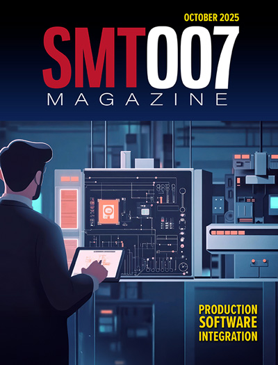
Production Software Integration
EMS companies need advanced software systems to thrive and compete. But these systems require significant effort to integrate and deploy. What is the reality, and how can we make it easier for everyone?

Spotlight on India
We invite you on a virtual tour of India’s thriving ecosystem, guided by the Global Electronics Association’s India office staff, who share their insights into the region’s growth and opportunities.

Supply Chain Strategies
A successful brand is built on strong customer relationships—anchored by a well-orchestrated supply chain at its core. This month, we look at how managing your supply chain directly influences customer perception.
- Articles
- Columns
- Links
- Media kit
||| MENU - smt007 Magazine
Advanced Packaging Gets an Additive Upgrade
November 8, 2022 | Art Wall, NextFlexEstimated reading time: 2 minutes
The recent approval of the CHIPS Act has reignited the U.S. semiconductor industry and shone a spotlight on the intricacies involved in chip manufacturing. As new technological innovations—such as 5G, IoT, AI, automotive and high-performance computing—come to market, they’re pushing chip manufacturing and integration capabilities. They demand more performance which leads to added complexity in an already extremely complicated process. All this requires a fundamental shift in the way that semiconductors are manufactured and integrated.
It's no secret that many believe Moore’s Law, the standard basis for semiconductor innovation over the past 50 years, is reaching the end of its reign. With a need to continue shrinking the size of components, engineers are running into roadblocks based on the physical limitations of electronics manufacturing, packaging, and integration. As manufacturers, we’re tasked with finding new ways of improving electronics capabilities, specifically regarding speed and size.
One of the key strategic avenues that’s arisen is rethinking how we approach the packaging and integration of modern semiconductors. This has implications across the board for chip design, including how they are combined and how they communicate between the chips. Combining dissimilar chips into an integrated package, called heterogeneous integration, and including somewhat generic chip building blocks called chiplets, is quickly becoming necessary to keep pace with technology advancement.
Challenges in Traditional Packaging and Chip Interconnect
Printed circuit boards (PCBs) are the backbone of electronics, acting to connect integrated circuits (ICs) and discrete components to form a larger working circuit. Historically, individually packaged chips and components are mounted to a PCB and interconnected to deliver functionality.
Following this methodology, all the layers in a board act as separate interconnects, leaving the top and bottom of the board to place components. As the drive to miniaturize while simultaneously becoming more complex requires the addition of more components, this is where we’ll begin to see limitations.
An important part of the CHIPS Act was the recognition that not only does the United States need to make massive investments in chip-making facilities or foundries, but also to invest heavily in advanced packaging. Serving as the next step of combining or integrating these chips with novel approaches will be just as important in the innovation of U.S. semiconductor manufacturing capabilities. Some forms of this approach already exist through methodologies such as multi-chip modules or system-in-package (SIP), but more radical approaches are needed to deliver the required performance of the devices.
To read this entire article, which appeared in the November 2022 issue of SMT007 Magazine, click here.
Testimonial
"In a year when every marketing dollar mattered, I chose to keep I-Connect007 in our 2025 plan. Their commitment to high-quality, insightful content aligns with Koh Young’s values and helps readers navigate a changing industry. "
Brent Fischthal - Koh YoungSuggested Items
NOVOSENSE, UAES and Innoscience Advance Power Electronics for New Energy Vehicles
10/17/2025 | PRNewswireThe partnership focuses on developing next-generation intelligent integrated Gallium Nitride (GaN) products. Leveraging their combined expertise, the new devices will deliver more reliable GaN driving and protection features, enabling higher power density and paving the way for wider adoption in automotive systems.
Jabil Announces Board Transitions
10/17/2025 | JabilJabil Inc. announced that Executive Chairman of the Board of Directors Mark T. Mondello and Directors Kathleen A. Walters and Jamie Siminoff will not seek re-election at Jabil’s Annual Meeting of Stockholders in January 2026.
StenTech Strengthens Precision Parts Platform with AME Acquisition
10/17/2025 | StenTechStenTech, North America’s leading provider of SMT printing solutions and precision manufacturing, has announced the acquisition of Advanced Metal Etching, Inc. (AME), a recognized specialist in chemically etched and laser cut precision parts.
MKS’ Atotech, ESI to Participate in TPCA Show & IMPACT Conference 2025
10/17/2025 | MKS’ AtotechMKS Inc., a global provider of enabling technologies that transform our world, announced that its strategic brands Atotech (process chemicals, equipment, software, and services) and ESI (laser systems) will showcase their latest range of leading manufacturing solutions for printed circuit board (PCB) and package substrate manufacturing at the upcoming 26th TPCA Show 2025 to be held at the Taipei Nangang Exhibition Center from 22-24 October 2025.
Rehm Wins Mexico Technology Award for CondensoXLine with Formic Acid
10/17/2025 | Rehm Thermal SystemsModern electronics manufacturing requires technologies with high reliability. By using formic acid in convection, condensation, and contact soldering, Rehm Thermal Systems’ equipment ensures reliable, void-free solder joints — even when using flux-free solder pastes.


