


 Fresh PCB Concepts: Key Considerations for Reliability, Performance, and Compliance in PCBs
 Elementary Mr. Watson: Navigating RF—A Glide Path Approach to Design Success
 Designers Notebook: Layer Stackup Planning for RF Circuit Boards


Keysight Introduces Signal Integrity Simulation Software for Hardware Engineers
January 19, 2023 | Keysight Technologies, Inc.Estimated reading time: 1 minute
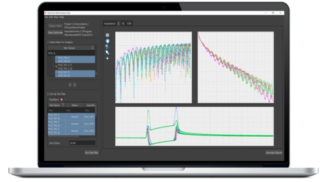
Keysight Technologies, Inc., a leading technology company that delivers advanced design and validation solutions to help accelerate innovation to connect and secure the world, introduces the Electrical Performance Scan (EP-Scan), a new high-speed digital simulation tool that supports rapid signal integrity (SI) analysis for hardware engineers and printed circuit board (PCB) designers.
After completing a PCB design, hardware engineers hand the design over to SI specialists to validate its performance before going to prototype. SI specialists perform simulations on a large number of nets, which can take days to weeks to complete. As a result, hardware engineers have difficulty predicting how much analysis time it will take to find errors or performance issues in the design. Uncertainty about the length of the SI analysis phase creates a bottleneck in the design cycle and delays time-to-market.
EP-Scan addresses SI analysis bottlenecks by giving hardware designers diagnostic tools to correct designs earlier and meet development schedules. As a stand-alone software product, EP-Scan performs electromagnetic (EM) simulation on signal nets and reports SI metrics such as channel return and insertion loss. In addition, EP-Scan automates performance comparisons between different versions of a design and generates simulation reports that expedite verification prior to building expensive physical prototypes.
"Our goal with EP-Scan is to 'shift left' the PCB design verification process by using early simulation to detect and correct errors, giving hardware designers the confidence to move forward and obtain first pass success," said Tim Wang-Lee, Ph.D., Product Marketing Manager at Keysight. "I am proud that EP-Scan is helping engineers to spend more time doing analyses to gain insights, documenting results to track progress, and automating routine tests. EP-Scan empowers hardware engineers by maximizing their productivity."
EP-Scan requires only the layout geometry and substrate stack-up information for the PCB design as inputs. After engineers specify the desired nets for investigation, EP-Scan reports simulation results including the characteristic impedance and delay of traces, return loss, insertion loss, and impedance time-domain reflectometry (TDR). By analyzing common fabrication formats such as ODB++, EP-Scan shows engineers the performance of their design as it would be when fabricated. EP-Scan enables hardware engineers to quickly validate designs and identify layout issues before the final verification, which reduces time-to-market, and can contribute to more PCB design wins.
Share on:


Suggested Items
Imec Coordinates EU Chips Design Platform
05/09/2025 | ImecA consortium of 12 European partners, coordinated by imec, has been selected in the framework of the European Chips Act to develop the EU Chips Design Platform.
New Issue of Design007 Magazine: Are Your Data Packages Less Than Ideal?
05/09/2025 | I-Connect007 Editorial TeamWhy is it so difficult to create the ideal data package? Many of these simple errors can be alleviated by paying attention to detail—and knowing what issues to look out for. So, this month, our experts weigh in on the best practices for creating the ideal data package for your design.
RF PCB Design Tips and Tricks
05/08/2025 | Cherie Litson, EPTAC MIT CID/CID+There are many great books, videos, and information online about designing PCBs for RF circuits. A few of my favorite RF sources are Hans Rosenberg, Stephen Chavez, and Rick Hartley, but there are many more. These PCB design engineers have a very good perspective on what it takes to take an RF design from schematic concept to PCB layout.
Cadence Unveils Millennium M2000 Supercomputer with NVIDIA Blackwell Systems
05/08/2025 | Cadence Design SystemsAt its annual flagship user event, CadenceLIVE Silicon Valley 2025, Cadence announced a major expansion of its Cadence® Millennium™ Enterprise Platform with the introduction of the new Millennium M2000 Supercomputer featuring NVIDIA Blackwell systems, which delivers AI-accelerated simulation at unprecedented speed and scale across engineering and drug design workloads.
The Right Blend: Mixed Wireless Technologies
05/08/2025 | Kirsten Zima, Siemens EDAA common trend recently is to employ as many radios as possible on a single PCB. With the increase of wireless standards and the downscaling of PCB size, it can be difficult to know what the most critical design parameters are to focus on. In this article, we’ll discuss the most important considerations to make when designing with mixed wireless technologies, such as Bluetooth, GPS, and Wi-Fi, on a single PCB. These considerations include antennas, frequencies, FCC compliance, shielding, and layout with and without transition vias.