-

- News
- Books
Featured Books
- design007 Magazine
Latest Issues
Current Issue
Signal Integrity
If you don’t have signal integrity problems now, you will eventually. This month, our expert contributors share a variety of SI techniques that can help designers avoid ground bounce, crosstalk, parasitic issues, and much more.

Proper Floor Planning
Floor planning decisions can make or break performance, manufacturability, and timelines. This month’s contributors weigh in with their best practices for proper floor planning and specific strategies to get it right.

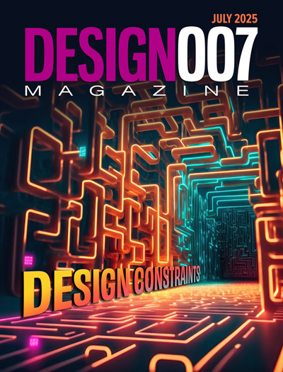
Showing Some Constraint
A strong design constraint strategy carefully balances a wide range of electrical and manufacturing trade-offs. This month, we explore the key requirements, common challenges, and best practices behind building an effective constraint strategy.
- Articles
- Columns
- Links
- Media kit
||| MENU - design007 Magazine
Imec Coordinates EU Chips Design Platform
May 9, 2025 | ImecEstimated reading time: 1 minute
A consortium of 12 European partners, coordinated by imec, has been selected in the framework of the European Chips Act to develop the EU Chips Design Platform. Funded by Chips JU, the platform will facilitate access to advanced semiconductor design infrastructure, training, and capital for fabless semiconductor startups, small and medium enterprises and research organizations. By providing the necessary resources, the initiative aims to democratize and foster semiconductor innovation across Europe, specifically for chip design.
The semiconductor industry is the backbone of modern technology, powering everything from smartphones to advanced medical devices. With the EU Chips Act, Europe is dedicated to increasing its global semiconductor market share. Next to the launch of European pilot lines that aim to develop key technologies for semiconductor innovation, the EU Chips Act has proposed the EU Chips Design Platform as a vehicle to support the growth of fabless chip companies in Europe.
The EU Chips Design Platform will enable fabless companies to access the resources they need quickly and efficiently via a cloud-based virtual environment, offering chip design resources, training, and capital. Coordinated by imec, twelve key European research players in the semiconductor ecosystem have joined forces in a consortium to create this design platform.
The platform aims to onboard the first startups and small and medium enterprises by early 2026, providing them with low-barrier access to European design capabilities, including route-to-chip fabrication, packaging, and testing. It will offer customized support to access commercial electronic design automation (EDA) tools, intellectual property (IP) libraries, EU Chips Act pilot line technologies, and access to design IP repositories, including open-source options. Additionally, the platform will feature a startup support program with incubation, acceleration, and mentoring activities next to financial assistance to help early-stage companies turn their innovative ideas into reality.
“The EU Chips Design Platform will provide crucial resources for startups and SMEs to accelerate their design journey and bring their business ideas to market faster. By reducing the barriers to access of design expertise, including EDA tools and IP, and drastically lowering chip design and fabrication costs and time-to-market, we will spark the growth of the European chip design industry,” stated Romano Hoofman, imec project coordinator.
Testimonial
"The I-Connect007 team is outstanding—kind, responsive, and a true marketing partner. Their design team created fresh, eye-catching ads, and their editorial support polished our content to let our brand shine. Thank you all! "
Sweeney Ng - CEE PCBSuggested Items
Mouser Electronics Celebrates Its 2025 Best-in-Class Award Winners
10/01/2025 | BUSINESS WIREMouser Electronics, Inc., the New Product Introduction (NPI) leader™ empowering innovation, is pleased to announce the 2025 recipients of the Mouser Best-in-Class Awards.
Elementary Mr. Watson: Chasing Checkmarks, Not Signal Integrity
10/01/2025 | John Watson -- Column: Elementary, Mr. WatsonFor the September 2025 issue of Design007 Magazine on signal integrity, I explored how the PCB is similar to a military obstacle course: walls that sap energy like impedance mismatches, barbed wire that cuts like crosstalk, and mud pits that drag a signal down like attenuation. The takeaway was clear that a PCB is not a flat drawing; it's an electromagnetic ecosystem filled with hazards that test every signal that dares to cross it. The real danger lies not in the obstacles themselves, but in the fact that many designers never see them.
Target Condition: Rethinking the PCB Stackup Recipe
10/01/2025 | Kelly Dack -- Column: Target ConditionMarie Antoinette is attributed with saying, “Let them eat cake,” but historians now agree she likely never said it. It was probably revolutionary propaganda to paint her as out of touch with the starving masses. Yet, the phrase still lingers, and oddly enough, it applies to the world of PCB design.
Siemens, ASE Collaborate on Workflows for ASE’s VIPack Advanced Packaging Platform
09/25/2025 | SiemensSiemens Digital Industries Software announced that it is collaborating with Advanced Semiconductor Engineering, Inc. (ASE), the leading global provider of semiconductor manufacturing services in assembly and test, to develop 3Dblox-based workflows for the ASE VIPack™ platform using Siemens’ Innovator3D IC™ solution, which is fully certified for the 3Dblox standard..
Cadence, TSMC Team on AI-Driven Flows and IP for Advanced Nodes, 3DFabric
09/25/2025 | BUSINESS WIRECadence announced major advancements in chip design automation and IP, driven by its long-standing relationship with TSMC to develop advanced design infrastructure and accelerate time to market, for AI and HPC customer applications.


