


 It’s Only Common Sense: Be the Vendor They Compare Everyone Else To
 The Marketing Minute: If Your Marketing Budget Gets Cut in Half, Then What?


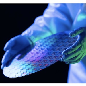
Siemens Digital Industries Software introduced Tessent™ Hi-Res Chain software, a new tool designed to address the critical challenges faced by integrated circuit (IC) design and manufacturing teams in advanced technology nodes, where even minor process variations can significantly impact yield and time-to-market.
As IC designs progress to more advanced nodes at 5nm and below, they become increasingly susceptible to manufacturing variations that can create defects and slow yield ramp. At these geometries, traditional failure analysis (FA) methods can require weeks or months of laboratory effort to investigate. Siemens’ new Tessent Hi-Res Chain tool addresses this problem by rapidly providing transistor-level isolation for scan chain defects. For advanced process nodes where yield ramp heavily relies on chain diagnosis, the new software can boost diagnosis resolution by more than 1.5x, reducing the need for costly extensive failure analysis cycles.
"Tessent Hi-Res Chain represents a major leap forward in our ability to rapidly identify and address yield-limiting factors in advanced IC designs," said Ankur Gupta, vice president and general manager of the Digital Design Creation Platform division, Siemens Digital Industries Software. "By providing unprecedented accuracy and resolution in defect isolation, we're empowering our customers to accelerate their yield ramp and improve time-to-market for cutting-edge semiconductor products."
By correlating design information and failure data from manufacturing tests with patterns from Tessent automatic test pattern generation (ATPG), Tessent Hi-Res Chain transforms failing test cycles into actionable insights. The solution employs layout-aware and cell-aware technology to pinpoint a defect's most probable failure mechanism, logic location, and physical location.
Tessent Hi-Res Chain builds on Siemens' market-leading chain diagnosis capabilities, offering precise defect isolation, even for point defects deep within design control signal networks.
The new solution maintains Tessent industry-leading accuracy rate, with over 80 percent of its generated reports consistently confirmed through FA processes using Tessent technology. This high level of reliability has made Tessent the go-to solution for yield ramping across multiple technology nodes.
Tessent Hi-Res Chain is part of Siemens' comprehensive Tessent product family, which offers best-in-class solutions for IC test, functional monitoring, and silicon lifecycle management. These tools work in concert to provide the highest test coverage, accelerate yield ramp, and improve quality and reliability throughout the silicon lifecycle.


