-

- News
- Books
Featured Books
- smt007 Magazine
Latest Issues
Current Issue
What's Your Sweet Spot?
Are you in a niche that’s growing or shrinking? Is it time to reassess and refocus? We spotlight companies thriving by redefining or reinforcing their niche. What are their insights?

Moving Forward With Confidence
In this issue, we focus on sales and quoting, workforce training, new IPC leadership in the U.S. and Canada, the effects of tariffs, CFX standards, and much more—all designed to provide perspective as you move through the cloud bank of today's shifting economic market.

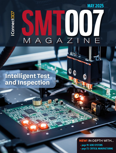
Intelligent Test and Inspection
Are you ready to explore the cutting-edge advancements shaping the electronics manufacturing industry? The May 2025 issue of SMT007 Magazine is packed with insights, innovations, and expert perspectives that you won’t want to miss.
- Articles
- Columns
- Links
- Media kit
||| MENU - smt007 Magazine
ZESTRON South Asia releases whitepaper – Impact of Cleaning Technology on Discrete Packaging - The Difference in Wire Bonding Yield
December 2, 2024 | ZESTRONEstimated reading time: 1 minute
ZESTRON, the global leading provider of high precision cleaning products, services, and training solutions in the electronics manufacturing and semiconductor industries, is pleased to release the whitepaper “Impact of Cleaning Technology on Discrete Packaging - The Difference in Wire Bonding Yield”
Whitepaper Abstract:
Lead frame packages are commonly used in semiconductor package fabrication, where interconnections between the integrated circuits (IC) and the metal leads are typically established through die attach and wire bonding processes. Standard materials like epoxies, adhesives, or solder pastes are most often used in the die attach process. However, it is critical to remove any flux residues left behind after soldering before proceeding with wire bonding and molding to ensure maximum yield in packages that use solder paste for die attachment. One of the most widely used cleaning agents to remove flux residues is isopropyl alcohol (IPA). While IPA is commonly used as a general cleaner in the electronics industry, it is not the most effective solution for flux removal.
Semiconductor package manufacturers produce millions of units daily and therefore, a small improvement in the wire bonding yield can significantly impact production efficiency and the overall product costs.
One such OEM was producing lead frame packages and using IPA (Isopropyl alcohol) in the ultrasonic cleaning process. However, their process resulted in a wire bonding yield of only 98%, measured after the molding and deflashing processes. This indicated significant motivation to improve the cleaning process and the wire bonding yield.
A Design of Experiment (DOE) was developed to assess alternative cleaning agents and process equipment, aiming to optimize the cleaning process and to be evaluated based on the improvement in wire bonding yield. Process qualification was conducted through a pull test according to the MIL-STD-883E method 2011.7. Throughout the DOE process iterations, process improvements were identified through visual inspection, pull and shear testing as well as overall yield measurement from the wire bonding process.
Testimonial
"The I-Connect007 team is outstanding—kind, responsive, and a true marketing partner. Their design team created fresh, eye-catching ads, and their editorial support polished our content to let our brand shine. Thank you all! "
Sweeney Ng - CEE PCBSuggested Items
Designers Notebook: Basic PCB Planning Criteria—Establishing Design Constraints
07/22/2025 | Vern Solberg -- Column: Designer's NotebookPrinted circuit board development flows more smoothly when all critical issues are predefined and understood from the start. As a basic planning strategy, the designer must first consider the product performance criteria, then determine the specific industry standards or specifications that the product must meet. Planning also includes a review of all significant issues that may affect the product’s manufacture, performance, reliability, overall quality, and safety.
Marcy’s Musings: From Pitch to PO—The Sales Stack
07/21/2025 | Marcy LaRont -- Column: Marcy's MusingsIt is a foundational truth that a company lives and dies by its sales. Receiving that PO or contract starts the operational chain. It is the purest symbol of the machinations of the business process: You are paying me for something I am doing, making, or sourcing for you. Then, every single thing a business does in executing and fulfilling that sales agreement speaks directly to customer experience and whether more POs will follow. You won't keep customers if you don't make a quality product and provide strong customer service.
July 2025 PCB007 Magazine: Sales—From Pitch to PO
07/18/2025 |Though all parts of a company are essential for holistic success, it is a foundational truth that a company lives and dies by its sales. If there are no sales, the company eventually ceases to exist, or as Henry Ford says, “Nothing happens until someone sells something.” In the July issue of PCB007 Magazine, we break down the sales stack and provide a guide to up your sales game.
Tightening of LPDDR4X Supply Drives Up Prices; Smartphone Brands to Accelerate Adoption of LPDDR5X
07/17/2025 | TrendForceTrendForce’s latest investigations reveal that major Korean and U.S. memory suppliers are expected to significantly reduce or even cease production of LPDDR4X in 2025 and 2026.
Beyond Design: Refining Design Constraints
07/17/2025 | Barry Olney -- Column: Beyond DesignBefore starting any project, it is crucial to develop a thorough plan that encompasses all essential requirements. This ensures that the final product not only aligns with the design concept but is also manufacturable, reliable, and meets performance expectations. High-speed PCB design requires us to not only push technological boundaries but also consider various factors related to higher frequencies, faster transition times, and increased bandwidths during the design process.


