-

- News
- Books
Featured Books
- design007 Magazine
Latest Issues
Current Issue
Showing Some Constraint
A strong design constraint strategy carefully balances a wide range of electrical and manufacturing trade-offs. This month, we explore the key requirements, common challenges, and best practices behind building an effective constraint strategy.

All About That Route
Most designers favor manual routing, but today's interactive autorouters may be changing designers' minds by allowing users more direct control. In this issue, our expert contributors discuss a variety of manual and autorouting strategies.

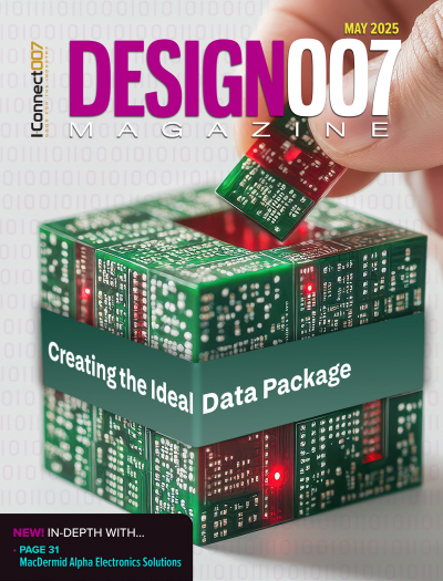
Creating the Ideal Data Package
Why is it so difficult to create the ideal data package? Many of these simple errors can be alleviated by paying attention to detail—and knowing what issues to look out for. So, this month, our experts weigh in on the best practices for creating the ideal design data package for your design.
- Articles
- Columns
- Links
- Media kit
||| MENU - design007 Magazine
Effects of Advanced Packaging and Stackup Design
December 26, 2024 | I-Connect007 Editorial TeamEstimated reading time: 1 minute
Kris Moyer teaches several PCB design classes for IPC and Sacramento State, including advanced PCB design. His advanced design classes take on some really interesting topics, including the impact of a designer’s choice of advanced packaging upon the design of the layer stackup.
Kris shares his thoughts on the relationship between packaging and stackup, what PCB designers need to know, and why he believes, “The rules we used to live by are no longer valid.”
Kris, tell us how advanced packaging can impact stackup design. What challenges do designers need to be aware of?
Kris Moyer: With advanced packaging you usually need to use HDI or UHDI technology. This usually means sequential lamination. With sequential lamination you need to select materials that can survive multiple lamination thermal cycles.
When we were discussing advanced packaging and stackup design recently, you said, “The rules we used to live by are no longer valid.” Expand on that a little bit.
As I mentioned, your selection of materials is now further restricted by the need for materials that survive multiple lamination cycles. Additionally, since we are adding layers one at a time and need plating on all layers, not just the outer layers, the copper design is now more difficult. Also, since we are adding layers one at a time, we can now have some select instances of unbalanced Z-axis and still meet bow and twist. Furthermore, many of the ultra-thin dielectric layers used in HDI/UHDI are just resin-coated copper without any reinforcement, so CTE/FA can be more of an issue.
To read this entire conversation, which appeared in the December 2024 issue of Design007 Magazine, click here.
Testimonial
"In a year when every marketing dollar mattered, I chose to keep I-Connect007 in our 2025 plan. Their commitment to high-quality, insightful content aligns with Koh Young’s values and helps readers navigate a changing industry. "
Brent Fischthal - Koh YoungSuggested Items
Setting Design Constraints Effectively
07/31/2025 | Stephen V. Chavez, Siemens EDAPCB design requires controlling energy within the medium of a PCB. The manner in which we control the chaos of energy is by implementing and utilizing physical and electrical rules, known as constraints, along with a specific structure and material(s) that make up what is known as the foundation of the design. These rules govern everything within the PCB structure and generally fall into two camps: performance and manufacturability. Setting this foundation correctly is extremely important and the key to success.
MacDermid Alpha Electronics Solutions Unveils Unified Global Website to Deepen Customer, Talent, and Stakeholder Engagement
07/31/2025 | MacDermid Alpha Electronics SolutionsMacDermid Alpha Electronics Solutions, the electronics business of Elements Solutions Inc, today launched macdermidalpha.com - a unified global website built to deepen digital engagement. The launch marks a significant milestone in the business’ ongoing commitment to delivering more meaningful, interactive, and impactful experiences for its customers, talent, and stakeholders worldwide.
Ansys 2025 R2 Enables Next-Level Productivity by Leveraging AI, Smart Automation, and Broader On-Demand Capabilities
07/30/2025 | PRNewswireAnsys, now part of Synopsys, announced 2025 R2, featuring new AI-powered capabilities across the portfolio that accelerate simulation and expand accessibility.
Connect the Dots: Sequential Lamination in HDI PCB Manufacturing
07/31/2025 | Matt Stevenson -- Column: Connect the DotsAs HDI technology becomes mainstream in high-speed and miniaturized electronics, understanding the PCB manufacturing process can help PCB design engineers create successful, cost-effective designs using advanced technologies. Designs that incorporate blind and buried vias, boards with space constraints, sensitive signal integrity requirements, or internal heat dissipation concerns are often candidates for HDI technology and usually require sequential lamination to satisfy the requirements.
Target Condition: The 5 Ws of PCB Design Constraints
07/29/2025 | Kelly Dack -- Column: Target ConditionHave you ever sat down to define PCB design constraints and found yourself staring at a settings window with more checkboxes than a tax form? You’re not alone. For many designers—especially those newer to the layout world—the task of setting up design constraints can feel like trying to write a novel in a language you just started learning.


