


 Knocking Down the Bone Pile: Revamp Your Components with BGA Reballing
 Global Sourcing Spotlight: Balancing Speed and Flexibility Without Sacrificing Control
 SMT Perspectives & Prospects: Artificial Intelligence Part 6: Data Module 1


Dorigo Systems Installs Koh Young 3D SPI, AOI Inspection Systems
July 23, 2015 | Koh Young TechnologyEstimated reading time: 2 minutes
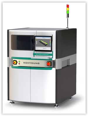
Canadian Pacific Northwest EMS leader Dorigo Systems has installed Koh Young KY8030-3 SPI and Zenith 3D AOI systems in their newest SMT PCBA manufacturing line, adding 3D measurement and inspection capability for printed solder paste (SPI) as well as completed SMT assemblies (AOI). Both systems are intended to optimize productivity and ensure product quality through process optimization through Koh Young’s patented measurement and inspection technologies. Dorigo is a thriving EMS provider with two manufacturing facilities totaling over 45,000 square feet located in Burnaby, British Columbia, Canada.
The combination of KY8030-3 SPI and Zenith AOI inspection solutions provides comprehensive defect prevention and yield improvement tools for Dorigo Systems to ensure that optimum quality is built into their products. Koh Young is the market leader for full 3D Solder Paste Inspection (SPI) and 3D Automated Optical Inspection (AOI) of SMT PCB assemblies.
“At any given time, we typically have over 300 open production jobs at our two operating plants, utilizing a wide variety of processes and equipment, and servicing the production requirements of more than 30 active customers,” says Mark Pillon, P. Eng., company President.. “It’s essential that our production process is optimized so that we can ship the highest quality defect-free product all the time with minimal process issues in our high-mix environment. We’re confident that these new Koh Young systems will help our production maintain its competitive edge.”
Koh Young’s KY8030-3 true 3D SPI measurement system provides full patented 3D measurement for the complete range of solder paste measurement and inspection across a wide measurement range while ensuring accuracy without sacrificing resolution.
With its authentic 3D measurement capability, Koh Young’s Zenith AOI system can detect all types of defects with real measurement values, allowing much easier defect evaluation and process control.
About Koh Young Technology
Koh Young Technology specializes in the design and manufacturing of 3D measurement and inspection equipment for the global circuit board assembly and semiconductor markets. Direct sales and support centers are located in the United States, Europe, Japan, Singapore, China (Shenzhen) and Korea. For more information about the company, visit www.kohyoung.com; contact the main office at 6150 W. Chandler Blvd., Suite #39, Chandler, AZ 85226. Office Tel: (480) 403-5000.
About Dorigo Systems Ltd.
Dorigo Systems is one of the Pacific Northwest’s leading contract manufacturers of Printed Circuit Board Assemblies (PCBAs). Dorigo’s mission is to manufacture the highest quality electronics using fast turnaround and dedicated service capabilities. Dorigo cost-effectively takes a customer’s product from prototype to full production, and Dorigo’s state-of-the-art circuit board manufacturing, can handle the most complicated and demanding projects. Contact the company at 3885 Henning Drive, Burnaby, BC V5C 6N5 Canada, Tel: 604-294-4600, email sales@dorigo.com or visit www.dorigo.com for more information.
Share on:


Testimonial
"The I-Connect007 team is outstanding—kind, responsive, and a true marketing partner. Their design team created fresh, eye-catching ads, and their editorial support polished our content to let our brand shine. Thank you all! "
Sweeney Ng - CEE PCBSuggested Items
Rehm Wins Mexico Technology Award for CondensoXLine with Formic Acid
10/17/2025 | Rehm Thermal SystemsModern electronics manufacturing requires technologies with high reliability. By using formic acid in convection, condensation, and contact soldering, Rehm Thermal Systems’ equipment ensures reliable, void-free solder joints — even when using flux-free solder pastes.
Indium Experts to Deliver Technical Presentations at SMTA International
10/14/2025 | Indium CorporationAs one of the leading materials providers to the power electronics assembly industry, Indium Corporation experts will share their technical insight on a wide range of innovative solder solutions at SMTA International (SMTAI), to be held October 19-23 in Rosemont, Illinois.
Knocking Down the Bone Pile: Revamp Your Components with BGA Reballing
10/14/2025 | Nash Bell -- Column: Knocking Down the Bone PileBall grid array (BGA) components evolved from pin grid array (PGA) devices, carrying over many of the same electrical benefits while introducing a more compact and efficient interconnect format. Instead of discrete leads, BGAs rely on solder balls on the underside of the package to connect to the PCB. In some advanced designs, solder balls are on both the PCB and the BGA package. In stacked configurations, such as package-on-package (PoP), these solder balls also interconnect multiple packages, enabling higher functionality in a smaller footprint.
Indium to Showcase High-Reliability Solder and Flux-Cored Wire Solutions at SMTA International
10/09/2025 | Indium CorporationAs one of the leading materials providers in the electronics industry, Indium Corporation® will feature its innovative, high-reliability solder and flux-cored wire products at SMTA International (SMTAI), to be held October 19-23 in Rosemont, Illinois.
‘Create your Connections’ – Rehm at productronica 2025 in Munich
10/08/2025 | Rehm Thermal SystemsThe electronics industry is undergoing dynamic transformation: smart production lines, sustainability, artificial intelligence, and sensor technologies dominate current discussions.