


 The Right Approach: I Hear the Train A Comin'
 It’s Only Common Sense: OCCAM—the Time Is Now
 Marcy's Musings: The Growing Industry
Nanotech Tools Open Market for More Miniature Electronics
October 29, 2015 | PICSEstimated reading time: 2 minutes
New methods for mass producing ultra-miniature capacitors could lead to new innovations in sectors ranging from medical tools to aeronautics.
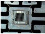
In order to develop ultra-miniaturised electronic components, ultra-miniaturised capacitors are required. The two-year EU-funded PICS project has developed tools that could soon lead to the mass production of high-density 3D integrated silicon capacitors, creating new opportunities for SMEs to tap demand for miniaturised high performance electronics across a range of sectors.
Capacitors are found in electronic components. Their role is to deliver power from a single source (such as a battery) – at the correct voltage level – in order for the component to carry out its different functions. Capacitors also protect electronic components against voltage jumps.
There is increasing demand from numerous high-growth high–value sectors, such as medicine, automotive, personal electronics and aeronautics, for applications based on smart and miniaturised sensors. These applications require electronic modules where size, reliability and performance are of equal importance.
The key long term objective of the project, which was completed at the end of August 2015, was to establish a cost effective industrial solution for developing ultra-miniaturised capacitors. Three SMEs joined forces with two research institutes in order to target the specific needs of end users such as aeronautics and medical instruments. Thanks to these partnerships, financial viability was ensured by focusing on the need for mass production.
Nanomedicine is another sector that is rapidly progressing from being primarily research-oriented to delivering measurable results and benefits to patients. The PICS consortium sought to develop high-end integrated capacitors for medical applications, along with the future DRAM market (DRAM is a type of random accessible memory used in various electronic devices such as PCs, smartphones, music players, laptops, netbooks, and tablets). The next step will be to commercially exploit the production innovations developed throughout the project.
A second long term objective of the project was to boost the potential of European SMEs operating within a high-value sector that promises significant growth potential. All three SMEs involved in PICS have benefited through the development of industry contacts and achieved a better understanding of end user needs. The project SMEs were also able to outsource some of their research in order to acquire cutting-edge technological know-how, which will enable them to better exploit their findings in the market place.
In terms of technological innovation, the project developed innovative atomic layer deposition (ALD) materials and tools in order to facilitate the mass production of high density and high voltage capacitors. ALD is a nanotechnology that allows ultra-thin films of just a few nanometres to be deposited in a precisely controlled way. This offers many benefits in semiconductor engineering. The tools developed by the PICS consortium enable 3D structures to be arranged.
A new process for accurately etching nanomaterials was also demonstrated by one of the SMEs, in collaboration with a leading research institute. This technique could be of interest for a number of different applications such as LED lighting and magnetic data storage.
Share on:


Suggested Items
Warm Windows and Streamlined Skin Patches – IDTechEx Explores Flexible and Printed Electronics
04/26/2024 | IDTechExFlexible and printed electronics can be integrated into cars and homes to create modern aesthetics that are beneficial and easy to use. From luminous car controls to food labels that communicate the quality of food, the uses of this technology are endless and can upgrade many areas of everyday life.
Book Excerpt: The Printed Circuit Assembler’s Guide to... Factory Analytics
04/24/2024 | I-Connect007 Editorial TeamIn our fast-changing, deeply competitive, and margin-tight industry, factory analytics can be the key to unlocking untapped improvements to guarantee a thriving business. On top of that, electronics manufacturers are facing a tremendous burden to do more with less. If you don't already have a copy of this book, what follows is an excerpt from the introduction chapter of 'The Printed Circuit Assembler’s Guide to... Factory Analytics: Unlocking Efficiency Through Data Insights' to whet your appetite.
Listen Up! The Intricacies of PCB Drilling Detailed in New Podcast Episode
04/25/2024 | I-Connect007In episode 5 of the podcast series, On the Line With: Designing for Reality, Nolan Johnson and Matt Stevenson continue down the manufacturing process, this time focusing on the post-lamination drilling process for PCBs. Matt and Nolan delve into the intricacies of the PCB drilling process, highlighting the importance of hole quality, drill parameters, and design optimization to ensure smooth manufacturing. The conversation covers topics such as drill bit sizes, aspect ratios, vias, challenges in drilling, and ways to enhance efficiency in the drilling department.
Elevating PCB Design Engineering With IPC Programs
04/24/2024 | Cory Blaylock, IPCIn a monumental stride for the electronics manufacturing industry, IPC has successfully championed the recognition of the PCB Design Engineer as an official occupation by the U.S. Department of Labor (DOL). This pivotal achievement not only underscores the critical role of PCB design engineers within the technology landscape, but also marks the beginning of a transformative journey toward nurturing a robust, skilled workforce ready to propel our industry into the future.
Winner of The Science Show Rakett 69 Receives Incap Scholarship
04/24/2024 | IncapThe winner of the Rakett 69 science show, Andri Türkson, who stood out as an electronics enthusiast, received a scholarship from Incap Estonia, along with an internship opportunity in Saaremaa.