


 The Right Approach: I Hear the Train A Comin'
 It’s Only Common Sense: OCCAM—the Time Is Now
 Marcy's Musings: The Growing Industry
Building Blocks for GaN Power Switches
December 28, 2015 | AIP.orgEstimated reading time: 4 minutes
A team of engineers from Cornell University, the University of Notre Dame and the semiconductor company IQE has created gallium nitride (GaN) power diodes capable of serving as the building blocks for future GaN power switches — with applications spanning nearly all electronics products and electricity distribution infrastructures.
Power semiconductor devices are a critical part of the energy infrastructure — all electronics rely on them to control or convert electrical energy. Silicon-based semiconductors are rapidly approaching their performance limits within electronics, so materials such as GaN are being explored as potential replacements that may render silicon switches obsolete.
But along with having many desirable features as a material, GaN is notorious for its defects and reliability issues. So the team zeroed in on devices based on GaN with record-low defect concentrations to probe GaN’s ultimate performance limits for power electronics. They describe their results in a paper in the journal Applied Physics Letters, from AIP Publishing.
“Our engineering goal is to develop inexpensive, reliable, high-efficiency switches to condition electricity — from where it’s generated to where it’s consumed within electric power systems — to replace generations-old, bulky, and inefficient technologies,” said Zongyang Hu, a postdoc working in Professor Grace Huili Xing’s research group within the School of Electrical and Computer Engineering at Cornell University. “GaN-based power devices are enabling technologies to achieve this goal.”
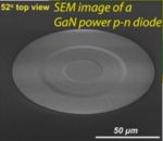
The team examined semiconductor p-n junctions, made by joining p-type (free holes) and n-type (free electrons) semiconductor materials, which have direct applications in solar cells, light-emitting diodes (LEDs), rectifiers in circuits, and numerous variations in more complex devices such as power transistors. “For our work, high-voltage p-n junction diodes are used to probe the material properties of GaN,” Hu explained.
To describe how much the device’s current-voltage characteristics deviate from the ideal case in a defect-free semiconductor system, the team uses a “diode ideality factor.” This is “an extremely sensitive indicator of the bulk defects, interface and surface defects, and resistance of the device,” he added.
Defects exist within all materials, but at varying levels. “So one parameter we used to effectively describe the defect level in a material is the Shockley-Read-Hall (SRH) recombination lifetime,” Hu said.
Page 1 of 2
Share on:


Suggested Items
Warm Windows and Streamlined Skin Patches – IDTechEx Explores Flexible and Printed Electronics
04/26/2024 | IDTechExFlexible and printed electronics can be integrated into cars and homes to create modern aesthetics that are beneficial and easy to use. From luminous car controls to food labels that communicate the quality of food, the uses of this technology are endless and can upgrade many areas of everyday life.
Book Excerpt: The Printed Circuit Assembler’s Guide to... Factory Analytics
04/24/2024 | I-Connect007 Editorial TeamIn our fast-changing, deeply competitive, and margin-tight industry, factory analytics can be the key to unlocking untapped improvements to guarantee a thriving business. On top of that, electronics manufacturers are facing a tremendous burden to do more with less. If you don't already have a copy of this book, what follows is an excerpt from the introduction chapter of 'The Printed Circuit Assembler’s Guide to... Factory Analytics: Unlocking Efficiency Through Data Insights' to whet your appetite.
Listen Up! The Intricacies of PCB Drilling Detailed in New Podcast Episode
04/25/2024 | I-Connect007In episode 5 of the podcast series, On the Line With: Designing for Reality, Nolan Johnson and Matt Stevenson continue down the manufacturing process, this time focusing on the post-lamination drilling process for PCBs. Matt and Nolan delve into the intricacies of the PCB drilling process, highlighting the importance of hole quality, drill parameters, and design optimization to ensure smooth manufacturing. The conversation covers topics such as drill bit sizes, aspect ratios, vias, challenges in drilling, and ways to enhance efficiency in the drilling department.
Elevating PCB Design Engineering With IPC Programs
04/24/2024 | Cory Blaylock, IPCIn a monumental stride for the electronics manufacturing industry, IPC has successfully championed the recognition of the PCB Design Engineer as an official occupation by the U.S. Department of Labor (DOL). This pivotal achievement not only underscores the critical role of PCB design engineers within the technology landscape, but also marks the beginning of a transformative journey toward nurturing a robust, skilled workforce ready to propel our industry into the future.
Winner of The Science Show Rakett 69 Receives Incap Scholarship
04/24/2024 | IncapThe winner of the Rakett 69 science show, Andri Türkson, who stood out as an electronics enthusiast, received a scholarship from Incap Estonia, along with an internship opportunity in Saaremaa.