


 It’s Only Common Sense: Nice Guys Really Can Finish First
 The Right Approach: I Hear the Train A Comin'
 Marcy's Musings: The Growing Industry
CPI Enhances Printed Electronics Capability; Installs NovaCentrix PulseForge
January 5, 2016 | Centre for Process Innovation (CPI)Estimated reading time: 3 minutes
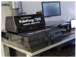
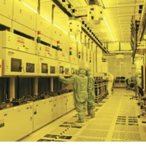
The Centre for Process Innovation (CPI) has recently partnered with NovaCentrix to install a specialist system designed for the high speed photonic curing of printed electronics inks. The NovaCentrix PulseForge 1300 state-of-the-art system is the first of its kind in the UK to be available to clients on an open access basis and will aid the commercialisation of a host of applications including printed sensing and Radio Frequency Identification (RFID) and Near Field Communication (NFC) antennas for smart packaging. The recent installation builds upon CPI’s existing capability for the market adoption of printed sensing technologies, allowing companies to develop and scale up their concepts from laboratory scale right through to pilot production.
Photonic curing has become a critical process in the manufacture of printed electronics products as very little energy is needed to sinter the inks to a high temperature. This allows for printed circuits to be produced on inexpensive and flexible materials such as plastic, paper or cardboard, whilst achieving excellent conductivity and without causing thermal damage to these materials. The technology is ideal for a number of printed electronics based applications that utilise low cost substrates such as printed temperature, capacitive touch and medical sensors, in addition to wearable electronics, energy harvesting devices and intelligent packaging products.
The NovaCentrix PulseForge tool at CPI uses specialist computer controlled high-intensity pulsed light technology enabling conductive inks to be sintered or annealed in a matter of milliseconds. The tool also provides the opportunity for comparably low cost inks formulated from copper-oxide and the rapid development of new printable electronics applications. Processing developed with the PulseForge 1300 at CPI can immediately be applied to volume production using the PulseForge platforms already in use for manufacturing of products sold world-wide.
New opportunities are opening up to integrate high volume, low cost printed sensors into everyday products with applications in a number of market sectors. The ‘Internet of Things’ and NFC are increasingly gathering attention from businesses, technology providers and most importantly the modern day consumer. NFC allows consumers to intuitively communicate with everyday items such as product packaging and sensors. The printing of electronic functionality has enabled product designers to embed electronic technology into their designs, creating innovative products that are low cost, smarter, lightweight and wireless. Applications are numerous, from interactive point-of-sale products and branding to disposable printed bio-sensors used in medical analysis and unobtrusive printed smart labels that allow for identification and anti-counterfeiting control. The integration of advanced printed sensors into paper and plastic opens up a wide range of market opportunities to create products with added value. Sensors can be designed to provide the opportunity to optimise logistics operations and stock control within the product life cycle and also to indicate the validity or quality of a product or whether the packaging has been subject to tampering during its transport and storage prior to purchase.
Page 1 of 2
Share on:


Suggested Items
All-Inclusive: PRIDE Industries Helps Employees With Disabilities to Succeed
05/01/2024 | Sandy Gentry, IPCPRIDE Industries is the leading employer of people with disabilities and those with other barriers to employment in the United States, including veterans and former foster youth. The company offers job training, placement, on-the-job coaching, and skills development for independent living. It has held IPC membership since 2000. Read more about this unique business and its connection to the electronics manufacturing industry.
TTM’s High Tech Expansion and Industry Innovation
04/30/2024 | Marcy LaRont, PCB007 MagazineTom Edman has been the CEO of TTM Technologies since 2014 and has an extensive background in electronics and manufacturing. TTM is a leading global manufacturer of technology solutions, including mission systems, RF component and RF microwave microelectronics assemblies, and quick turn and advanced technology printed circuit boards.
Latest Test and Inspection Solutions from GOEPEL electronic at SMTconnect 2024
04/29/2024 | GOEPEL electronicGOEPEL electronic will be demonstrating automated test and inspection equipment at SMTconnect, taking place in Nuremberg from June 11 to 13, 2024.
Arlon Electronic Materials Awarded Requalification to IPC-4101 QPL for All Polyimide Specification Sheets
04/29/2024 | IPCIPC's Validation Services Program has awarded Arlon Electronic Materials Division, an electronics material manufacturing company headquartered in Rancho Cucamonga, Calif., an IPC-4101 Qualified Products Listing (QPL) requalification for the third time.
Warm Windows and Streamlined Skin Patches – IDTechEx Explores Flexible and Printed Electronics
04/26/2024 | IDTechExFlexible and printed electronics can be integrated into cars and homes to create modern aesthetics that are beneficial and easy to use. From luminous car controls to food labels that communicate the quality of food, the uses of this technology are endless and can upgrade many areas of everyday life.