


 Dan’s Biz Bookshelf: ‘The Next RenAIssance: AI and the Expansion of Human Potential’
 The Chemical Connection: When the Industry Moves Faster Than the Standards
 Driving Innovation: Selecting the Right Laser Source


Quantum Dot Solids: This Generation's Silicon Wafer?
February 25, 2016 | Cornell UniversityEstimated reading time: 3 minutes
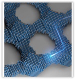
Just as the single-crystal silicon wafer forever changed the nature of electronics 60 years ago, a group of Cornell researchers is hoping its work with quantum dot solids – crystals made out of crystals – can help usher in a new era in electronics.
The multidisciplinary team, led by Tobias Hanrath, associate professor in the Robert Frederick Smith School of Chemical and Biomolecular Engineering, and graduate student Kevin Whitham, has fashioned two-dimensional superstructures out of single-crystal building blocks. Through directed assembly and attachment processes, the lead selenide quantum dots are synthesized into larger crystals, then fused together to form atomically coherent square superlattices.
The difference between these and previous crystalline structures is the atomic coherence of each 5-nanometer crystal (a nanometer is one-billionth of a meter). They’re not connected by a substance between each crystal – they’re connected directly to each other. The electrical properties of these superstructures potentially are superior to existing semiconductor quantum dots, with anticipated applications in solar cells and other electronic devices.
“As far as level of perfection, in terms of making the building blocks and connecting them into these superstructures, that is probably as far as you can push it,” Hanrath said, referring to the atomic-scale precision of the process.
The paper, “Charge transport and localization in atomically coherent quantum dot solids,” is published in the Feb. 22 issue of Nature Materials.
Whitham, a doctoral candidate in the field of materials science and engineering, did most of the experimentation and is lead author of the work. Also contributing were: Jun Yang, postdoctoral researcher; Benjamin H. Savitzky, graduate student in the field of physics; Lena Kourkoutis, assistant professor and Morgan Sesquicentennial Faculty Fellow in applied and engineering physics; and Frank Wise, the Samuel B. Eckert Professor of Engineering.
Provided
Associate professor Tobias Hanrath explains his group’s work on assembling quantum dots into ordered, two-dimensional superlattices, the subject of a paper published Feb. 22 in Nature Materials. The work has potential applications in optoelectronics.
This latest work has grown out of previous published research by the Hanrath group, including a 2013 paper published in Nano Letters that reported a new approach to connecting quantum dots through controlled displacement of a connector molecule, called a ligand. That paper referred to “connecting the dots” – i.e. electronically coupling each quantum dot – as being one of the most persistent hurdles to be overcome.
That barrier seems to have been cleared with this new research. The strong coupling of the quantum dots leads to formation of energy bands that can be manipulated based on the crystals’ makeup, and could be the first step toward discovering and developing other novel materials with programmable electronic structure.
Still, Whitham said, more work must be done to bring the group’s findings from the lab to technological fruition. The structure of the superlattice, while superior to ligand-connected quantum dot solids, still has multiple sources of disorder due to the fact that, in contrast to atoms in an ordinary solid, no two quantum dots are truly identical. This creates defects, which limits how far the electron wave function can spread.
“I see this paper as a challenge for other researchers to take this to another level,” Whitham said. “This is as far as we know how to push it now, but if someone were to come up with some technology, some chemistry, to provide another leap forward, this is challenging other people to say, ‘How can we do this better?’”
Hanrath said the discovery can be viewed in one of two ways, depending on whether you see the glass as half empty or half full.
“It’s the equivalent of saying, ‘Now we’ve made a really large single-crystal wafer of silicon, and access to high-quality samples yields new understanding and technological advances,’” he said, referencing the game-changing electronics discovery of the 1950s. “That’s the good part, but the potentially bad part of it is, we now have a better understanding that if you wanted to improve on our results, those challenges are going to be really, really difficult.”
This work made use of the Cornell Center for Materials Research, which is supported by the National Science Foundation (NSF) through its Materials Research Science and Engineering Center program. X-ray scattering was conducted at the Cornell High Energy Synchrotron Source, which is supported by the NSF and the National Institutes of Health.
Share on:


Subscribe
Stay ahead of the technologies shaping the future of electronics with our latest newsletter, Advanced Electronics Packaging Digest. Get expert insights on advanced packaging, materials, and system-level innovation, delivered straight to your inbox.Subscribe now to stay informed, competitive, and connected.
Suggested Items
Driving Innovation: Selecting the Right Laser Source
04/28/2026 | Simon Khesin -- Column: Driving InnovationWhen I first joined Schmoll Maschinen, I brought experience from almost every PCB process, except for laser. As I immersed myself in laser processing, I realized why it can seem so daunting to a newcomer. The complexity arises from three intersecting factors: A vast variety of laser sources: CO2, UV-nano, green-pico, UV-pico, IR-pico, and others; a diverse range of applications: Drilling, cutting, ablation, and more; and an extensive list of materials: These have vastly different absorption rates. Choosing the right machine or laser source is rarely trivial. Even for experienced engineers, answering "Which source is best?" requires examining the business's specific goals.
Insulectro: Advanced PCB Fabrication Materials
04/23/2026 | Real Time with... APEX EXPOExplore advanced PCB fabrication materials with Insulectro's Dain Hertsgaard and Gabriel Zepeda. This interview covers Arlon's innovative polyimide and epoxy solutions, including low-flow options for flex materials and high-performance materials for HDI applications; Qnity's polyimide films for demanding environments, and DuPont Interra's capacitance films for enhanced reliability. Insulectro offers comprehensive service and a commitment to advancing circuit technology
A Mic, a Tiny Cam, and the Show Floor: The Story Behind 'Take the Mic!'
04/23/2026 | I-Connect007 Editorial TeamI-Connect007’s Take the Mic! program at APEX EXPO 2026 in Anaheim is proving to be a must-watch feature for this year’s event coverage, as we invited company representatives to participate in a sponsored conversation about their businesses and products in a whole new way: in front of a camera at their booths. While our managing editors and guest editors were conducting slightly longer Real Time with… APEX EXPO interviews in our booth, three staff members and guests acted as roaming reporters, conducting short, prearranged interviews with several companies exhibiting on the show floor.
Target Condition: When Design Outpaces Manufacturing
04/23/2026 | Kelly Dack -- Column: Target ConditionMost PCB designers already understand why design for manufacturing (DFM) matters. If a product can’t be built reliably, repeatedly, and at a price anyone will actually pay, it’s dead on arrival. You may have the most elegant schematic and layout ever drawn in a CAD tool, but if the PCB suppliers can’t make it, or the EMS sources refuse to quote it, you may well be considered more of a Nutty Professor or well-meaning inventor than a PCB designer.
AGC's Advanced PCB Material Solutions
04/17/2026 | Real Time with... APEX EXPOAGC's line includes advanced PCB materials for critical industries such as aerospace, defense, and medical. This interview highlights their commitment to North American sourcing, offering solutions to today's challenges. AGC provides specialized automotive PCB materials including fastRise, a low-loss non-reinforced prepreg designed for high-frequency applications like 77 GHz radar.