


 Dan’s Biz Bookshelf: 'This Is Strategy: Make Better Plans'
 The Chemical Connection: Reducing Defects in Circuit Board Production
 It’s Only Common Sense: Trust Is All You Need


New LPKF Contac S4 for Galvanic Through-hole Plating
March 15, 2016 | LPKFEstimated reading time: 2 minutes
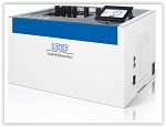
In the manufacturing of double-sided or multilayer PCBs, reliable electrical connection of the conductive networks is essential. At Embedded World in February 2016, LPKF will present the compact Contac S4 system for galvanic through-hole plating without the need for any knowledge of chemistry.
Complex electronic circuits have outgrown single-sided boards. The backs of the boards must also transmit current or signals; in addition, as complexity increases, the number of layers required also increases. Currently prototypes with up to eight layers can be produced in the lab. Various methods are available for connecting the layers.
Copper rivets can be used in a few cases for through holes with relatively large hole diameters. Copper rivets and punch tools with various diameters are available.
Another method uses a specially designed paste that is pulled through the holes by a vacuum and then cured in a furnace. Holes with diameters of up to 0.4 mm can be contacted reliably with a resistance of 20 mΩ.
The LPKF Contac S4 can be used for reliable, homogeneous through-hole plating of up to eight layers in the lab.
For assembly production prototypes, multilayers, and small holes with diameters of up to 0.2 mm, galvanic through-hole plating is the best option. In this process, holes are introduced into the unstructured base material, which is then given a conductive coating. The boards are electrically contacted and suspended in a galvanic bath. Copper is built up on every conductive surface in a galvanic process. The LPKF Contac S4 has six baths for performing all the necessary steps: activation, cleaning, and galvanization. In addition, tin plating can be performed in one of the baths to provide surface protection and improve solderability.
The LPKF Contac S4 underwent a number of changes from the predecessor models: A new anode plate design in conjunction with reverse pulse plating ensures highly homogeneous copper layer buildup with a layer tolerance of a mere ± 2 µm. Boards contacted in this way can be structured easily, e.g., with the LPKF ProtoLaser S4 (laser source in the green range of the visible light spectrum) without any damage being done to the organic substrate. A cleaning step for microvias also guarantees the quality of the contacts, even with fine holes with an aspect ratio of 1:10.
A new operating concept with a touch panel is being used for the first time in the LPKF Contac S4. The wizard guides the user through each step of the process and ensures that the process can be performed by any user, with or without any knowledge of chemistry.
The system requires very little maintenance and is made of high-quality discoloration-resistant materials.
About LPKF
Established in 1976, LPKF Laser & Electronics manufactures milling machines and laser systems used in circuit board and microelectronics fabrication, medical technology, the automotive sector, and the production of solar cells. LPKF’s worldwide headquarters is located in Hannover, Germany and its North American headquarters resides near Portland, Ore.
Share on:


Suggested Items
RF PCB Design Tips and Tricks
05/08/2025 | Cherie Litson, EPTAC MIT CID/CID+There are many great books, videos, and information online about designing PCBs for RF circuits. A few of my favorite RF sources are Hans Rosenberg, Stephen Chavez, and Rick Hartley, but there are many more. These PCB design engineers have a very good perspective on what it takes to take an RF design from schematic concept to PCB layout.
Trouble in Your Tank: Causes of Plating Voids, Pre-electroless Copper
05/09/2025 | Michael Carano -- Column: Trouble in Your TankIn the business of printed circuit fabrication, yield-reducing and costly defects can easily catch even the most seasoned engineers and production personnel off guard. In this month’s column, I’ll investigate copper plating voids with their genesis in the pre-plating process steps.
Elephantech: For a Greener Tomorrow
04/16/2025 | Marcy LaRont, PCB007 MagazineNobuhiko Okamoto is the global sales and marketing manager for Elephantech Inc., a Japanese startup with a vision to make electronics more sustainable. The company is developing a metal inkjet technology that can print directly on the substrate and then give it a copper thickness by plating. In this interview, he discusses this novel technology's environmental advantages, as well as its potential benefits for the PCB manufacturing and semiconductor packaging segments.
Trouble in Your Tank: Organic Addition Agents in Electrolytic Copper Plating
04/15/2025 | Michael Carano -- Column: Trouble in Your TankThere are numerous factors at play in the science of electroplating or, as most often called, electrolytic plating. One critical element is the use of organic addition agents and their role in copper plating. The function and use of these chemical compounds will be explored in more detail.
IDTechEx Highlights Recyclable Materials for PCBs
04/10/2025 | IDTechExConventional printed circuit board (PCB) manufacturing is wasteful, harmful to the environment and energy intensive. This can be mitigated by the implementation of new recyclable materials and technologies, which have the potential to revolutionize electronics manufacturing.