


 American Made Advocacy: Batting .333: Great in Baseball, Not in Microelectronics
 It’s Only Common Sense: The Best Cold Calling Ideas of All Times
 The Doctor’s In: Reliability in the Delivery Room
Recent Advances in Optical Materials
March 18, 2016 | ACN NewswireEstimated reading time: 1 minute
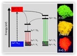
Japanese scientists have reviewed recent progress in advanced optical materials based on gadolinium aluminate garnet (GAG), while pointing out the knowledge gaps that need to be filled to improve their optical performance.
Their article, published in the open access journal Science and Technology of Advanced Materials, investigates the conditions in which GAG materials perform best. GAG is a synthetic material used in optics and crystal growth, as seeds to grow large crystals of similar materials.
Rare-earth aluminate garnets are an important family of multi-functional ceramic materials. They are useful in phosphors and lasers - often with medical applications such as cancer diagnosis and treatment. Researchers have tried to improve the chemical stability and luminescence of these materials and to understand their novel emission features.
In their review, Ji-Guang Li and Yoshio Sakka, of Japan's National Institute for Materials Science, discuss the ways to stabilise the GAG lattice and its performance in scintillators and "down-conversion phosphors", where high-energy photons are converted to low-energy ones.
Anti-site defects, where atoms of different types exchange their positions, are common in these materials. These can have profound effects on emissions as the atoms interact with excited electrons. This needs to be better understood, say the authors, in order to improve the overall performance of this class of optical materials.
Share on:


Suggested Items
AIM Solder Appoints Mhanny Aguillo as Southeast Asia Technical Sales Manager
05/31/2024 | AIMAIM Solder, a leading global manufacturer of solder assembly materials, is pleased to announce the appointment of Mhanny Aguillo as the Southeast Asia Technical Sales Manager.
Underconstraining Your Materials? Leave It to the Experts
05/30/2024 | I-Connect007 Editorial TeamWith traditional laminates now sporting improved resin systems, some OEMs are choosing various flavors of FR-4 instead of high-speed laminates for their high-speed designs—even RF applications. Avoiding overconstraining your materials in high-speed products can lead to considerable cost savings, not to mention a more streamlined trip through fabrication.
Elementary, Mr. Watson: Pushing Design Boundaries
05/29/2024 | John Watson -- Column: Elementary, Mr. WatsonOverconstraint: What a concept. Our first thoughts would be: What are we hurting by overconstraining a design? Isn't it better to be safe than sorry? What is meant by overconstraint? It means to apply excessive constraints. In engineering and mathematics, it's used when there are too many simultaneous equations to result in an exact solution. For example, fitting a line to many points is overconstrained because a line cannot be drawn simultaneously through all of the points. In PCB design, overconstraints always occur, including dimensional, electrical, manufacturing, and timing constraints. The list goes on.
Indium Corporation Expert to Present at MiNaPAD 2024
05/27/2024 | Indium CorporationIndium Corporation’s Senior Global Product Manager for Semiconductor and Advanced Materials, Sze Pei Lim, will deliver two technical presentations at the 11th Micro/Nano-Electronics Packaging and Assembly, Design and Manufacturing (MiNaPAD) Forum, taking place June 19-20 in Grenoble, France.
IDTechEx Asks if Silicon Anodes Are the Key to Mass EV Adoption
05/24/2024 | PRNewswireMaximizing energy density has been one key area of focus in electric vehicle battery development. Optimizations in cell and battery pack designs, alongside the use of higher nickel NMC and NCA cathodes, have led to steady improvement in battery energy density over the past 10-15 years.