


 Dan’s Biz Bookshelf: ‘Believe in Better'
 The Big Picture: Our Big ‘Why’ in the Age of AI
 The Chemical Connection: Through-glass Vias in Glass Substrates


The Future of Computer-Integrated Manufacturing in the PCB Industry
May 9, 2016 | Pete Starkey, I-Connect007Estimated reading time: 7 minutes
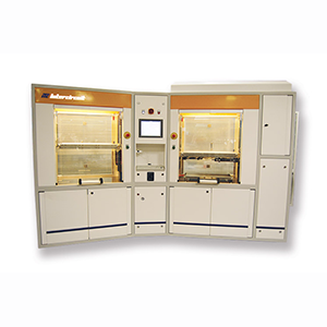
Computer-integrated manufacturing is already a proven reality in the PCB industry for those prepared to make the investment, and results in improved quality and reduced costs. The biggest barrier to its general adoption is the reluctance of some equipment manufacturers to communicate in a uniform data format. But trade associations such as TPCA are promoting cooperation and equipment suppliers are realising the benefits of uniformity, and that the long-term consequence of not cooperating is to be left out of the game. I sat down in the booth of Manz China Souzhou Ltd. During CPCA recently, and I spoke to Alex Liu, head of the PCB business unit, who explained the situation.
Pete Starkey: Alex, good morning and thank you for joining us. Alex, we are discussing computer-integrated manufacturing. Maybe you could explain to us how this fits into the PCB manufacturing process. What is the current state of the art? And what will be the developments going forward?
Alex Liu: Okay, so let me first explain why we first came up with this idea of computer-integrated manufacturing systems. The PCB manufacturing process is physically divided into different areas—some in the clean room, some is in the yellow-light area, and some in the plating areas, so how do we interconnect all the data? The first idea that we came up with was to use a computing system to interlink all of the signals and all of the parameter settings. Secondly, PCB manufacture relies heavily on labor to operate machines. And now, even in China, labor costs are getting higher and higher. And training costs are high also, not to mention that the people-exchange rates are very high in some areas, which means that the investment in operator experience is lost when people transfer. And thirdly, we are selling it as a packaged solution; we want to sell an integrated solution to the customer. So we should be able to connect all our systems into one so that the customer gets the best benefits. These were the three ideas behind our systems.
What most benefits the customer is having very easy access over the computing system. For example, if you are at a different manufacturing location, then you can easily use this system to have the same parameter settings, tracking, and a constant process, which will also improve your quality. So I think that’s a major benefit to the customer.
Starkey: If we take the PCB manufacturing process, typically where would you derive the information and where would you make the connections?
Liu: Our first product release is in the plating area, especially after de-smear, PTH and copper plating. Our system was first launched with a Korean customer. They want tracking of all the copper thicknesses being plated. So they have inspection feeding back to their data bank and their data bank will give references to compare to the original data. If they find something different, then their data bank will give us an instruction that will connect to our control system. And that will automatically change the manufacturing parameters on the line to improve the quality to reach their target.
Starkey: So, when we talk about manufacturing parameters in the context of a plating process, what specific parameters would you be measuring, recording, and feeding back?
Liu: Take plating, because our first project was in PTH. It's pretty thin copper, so you need a cross-section. Cross-sectioning cannot be in-line, you have to do it off-line. So once the quality control engineer has input the cross-section data to the system, the system automatically analyses what parameters resulted in this thickness of copper being plated. Of course the reference data was created by the customer as best-experience data and they would give us a recommendation that, for example, we should change the line speed, the spray, or whatever, and then we control the outcome and the results.
Starkey: So you can customize the system to suit the particular requirements of each customer at each stage of the manufacturing process.
Liu: Correct. I just mentioned that was our first approach. Our second approach was in the yellow-light area. We have our etching solutions and also we integrate with our LDI. As you may know, we merged with another company, KLEO in Germany, for LDI last year. So we are able to integrate from the imaging process until etching. We connect with the visual inspections system, taking the picture and then measuring the line space and width to verify that the etching results meet their requirements.
If not, they feedback a signal to us. We can easily change the parameters in the imaging system or the etching process. For example, we change the line speed, we change the spray or we activate the pneumatic etching or not. So we relay to the customer’s data bank so that they can give us the best recipe to create the pattern that they want. So that is the second approach that we have taken.
Then, combining these two projects, we found that we were able to connect the lines so they can export signals for us, then it's easier to control the whole line integrated into one. So for customers it's very easy. They just key in what kind of result they want, and everything is controlled by computing. It makes life really easy.
Page 1 of 2
Share on:


Suggested Items
The Evolution of Picosecond Laser Drilling
06/19/2025 | Marcy LaRont, PCB007 MagazineIs it hard to imagine a single laser pulse reduced not only from nanoseconds to picoseconds in its pulse duration, but even to femtoseconds? Well, buckle up because it seems we are there. In this interview, Dr. Stefan Rung, technical director of laser machines at Schmoll Maschinen GmbH, traces the technology trajectory of the laser drill from the CO2 laser to cutting-edge picosecond and hybrid laser drilling systems, highlighting the benefits and limitations of each method, and demonstrating how laser innovations are shaping the future of PCB fabrication.
Day 2: More Cutting-edge Insights at the EIPC Summer Conference
06/18/2025 | Pete Starkey, I-Connect007The European Institute for the PCB Community (EIPC) summer conference took place this year in Edinburgh, Scotland, June 3-4. This is the third of three articles on the conference. The other two cover Day 1’s sessions and the opening keynote speech. Below is a recap of the second day’s sessions.
Day 1: Cutting Edge Insights at the EIPC Summer Conference
06/17/2025 | Pete Starkey, I-Connect007The European Institute for the PCB Community (EIPC) Summer Conference took place this year in Edinburgh, Scotland, June 3-4. This is the second of three articles on the conference. The other two cover the keynote speeches and Day 2 of the technical conference. Below is a recap of the first day’s sessions.
Preventing Surface Prep Defects and Ensuring Reliability
06/10/2025 | Marcy LaRont, PCB007 MagazineIn printed circuit board (PCB) fabrication, surface preparation is a critical process that ensures strong adhesion, reliable plating, and long-term product performance. Without proper surface treatment, manufacturers may encounter defects such as delamination, poor solder mask adhesion, and plating failures. This article examines key surface preparation techniques, common defects resulting from improper processes, and real-world case studies that illustrate best practices.
RF PCB Design Tips and Tricks
05/08/2025 | Cherie Litson, EPTAC MIT CID/CID+There are many great books, videos, and information online about designing PCBs for RF circuits. A few of my favorite RF sources are Hans Rosenberg, Stephen Chavez, and Rick Hartley, but there are many more. These PCB design engineers have a very good perspective on what it takes to take an RF design from schematic concept to PCB layout.