


 The Right Approach: I Hear the Train A Comin'
 It’s Only Common Sense: OCCAM—the Time Is Now
 Marcy's Musings: The Growing Industry
Scientists Achieve Storage Memory Breakthrough
May 17, 2016 | IBMEstimated reading time: 4 minutes
For the first time, scientists at IBM Research have demonstrated reliably storing 3 bits of data per cell using a relatively new memory technology known as phase-change memory (PCM).
The current memory landscape spans from venerable DRAM to hard disk drives to ubiquitous flash. But in the last several years PCM has attracted the industry’s attention as a potential universal memory technology based on its combination of read/write speed, endurance, non-volatility and density. For example, PCM doesn’t lose data when powered off, unlike DRAM, and the technology can endure at least 10 million write cycles, compared to an average flash USB stick, which tops out at 3,000 write cycles.
This research breakthrough provides fast and easy storage to capture the exponential growth of data from mobile devices and the Internet of Things.
Applications
IBM scientists envision standalone PCM as well as hybrid applications, which combine PCM and flash storage together, with PCM as an extremely fast cache. For example, a mobile phone’s operating system could be stored in PCM, enabling the phone to launch in a few seconds. In the enterprise space, entire databases could be stored in PCM for blazing fast query processing for time-critical online applications, such as financial transactions.
Machine learning algorithms using large datasets will also see a speed boost by reducing the latency overhead when reading the data between iterations.
How PCM Works
PCM materials exhibit two stable states, the amorphous (without a clearly defined structure) and crystalline (with structure) phases, of low and high electrical conductivity, respectively.
To store a ‘0’ or a ‘1’, known as bits, on a PCM cell, a high or medium electrical current is applied to the material. A ‘0’ can be programmed to be written in the amorphous phase or a ‘1’ in the crystalline phase, or vice versa. Then to read the bit back, a low voltage is applied. This is how re-writable Blue-ray Discs* store videos.
Previously scientists at IBM and other institutes have successfully demonstrated the ability to store 1 bit per cell in PCM, but today at the IEEE International Memory Workshop in Paris, IBM scientists are presenting, for the first time, successfully storing 3 bits per cell in a 64k-cell array at elevated temperatures and after 1 million endurance cycles.
“Phase change memory is the first instantiation of a universal memory with properties of both DRAM and flash, thus answering one of the grand challenges of our industry,” said Dr. Haris Pozidis, an author of the paper and the manager of non-volatile memory research at IBM Research - Zurich. “Reaching 3 bits per cell is a significant milestone because at this density the cost of PCM will be significantly less than DRAM and closer to flash.”
To achieve multi-bit storage IBM scientists have developed two innovative enabling technologies: a set of drift-immune cell-state metrics and drift-tolerant coding and detection schemes.
More specifically, the new cell-state metrics measure a physical property of the PCM cell that remains stable over time, and are thus insensitive to drift, which affects the stability of the cell’s electrical conductivity with time. To provide additional robustness of the stored data in a cell over ambient temperature fluctuations a novel coding and detection scheme is employed. This scheme adaptively modifies the level thresholds that are used to detect the cell’s stored data so that they follow variations due to temperature change. As a result, the cell state can be read reliably over long time periods after the memory is programmed, thus offering non-volatility.
“Combined these advancements address the key challenges of multi-bit PCM, including drift, variability, temperature sensitivity and endurance cycling,” said Dr. Evangelos Eleftheriou, IBM Fellow.
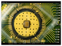
The experimental multi-bit PCM chip used by IBM scientists is connected to a standard integrated circuit board. The chip consists of a 2 × 2 Mcell array with a 4- bank interleaved architecture. The memory array size is 2 × 1000 μm × 800 μm. The PCM cells are based on doped-chalcogenide alloy and were integrated into the prototype chip serving as a characterization vehicle in 90 nm CMOS baseline technology.
OpenPOWER
At the 2016 OpenPOWER Summit in San Jose, CA, last month, IBM scientists demonstrated, for the first time, phase-change memory attached to POWER8-based servers (made by IBM and TYAN® Computer Corp.) via the CAPI (Coherent Accelerator Processor Interface) protocol. This technology leverages the low latency and small access granularity of PCM, the efficiency of the OpenPOWER architecture and the CAPI protocol. In the demonstration the scientists measured very low and consistent latency for 128-byte read/writes between the PCM chips and the POWER8 processor.
About IBM Research
For more than seven decades, IBM Research has defined the future of information technology with more than 3,000 researchers in 12 labs located across six continents. Scientists from IBM Research have produced six Nobel Laureates, 10 U.S. National Medals of Technology, five U.S. National Medals of Science, six Turing Awards, 19 inductees in the U.S. National Academy of Sciences and 20 inductees into the U.S. National Inventors Hall of Fame.
Share on:


Suggested Items
Warm Windows and Streamlined Skin Patches – IDTechEx Explores Flexible and Printed Electronics
04/26/2024 | IDTechExFlexible and printed electronics can be integrated into cars and homes to create modern aesthetics that are beneficial and easy to use. From luminous car controls to food labels that communicate the quality of food, the uses of this technology are endless and can upgrade many areas of everyday life.
iNEMI Packaging Tech Topic Series: Role of EDA in Advanced Semiconductor Packaging
04/26/2024 | iNEMIAdvanced semiconductor packaging with heterogenous integration has made on-package integration of multiple chips a crucial part of finding alternatives to transistor scaling. Historically, EDA tools for front-end and back-end design have evolved separately; however, design complexity and the increased number of die-to-die or die-to-substrate interconnections has led to the need for EDA tools that can support integration of overall design planning, implementation, and system analysis in a single cockpit.
Koh Young Showcases Award-winning Inspection Solutions at SMTconnect with SmartRep in Hall 4A.225
04/25/2024 | Koh Young TechnologyKoh Young Technology, the industry leader in True 3D measurement-based inspection solutions, will showcase an array of award-winning inspection and measurement solutions at SMTconnect alongside its sales partner, SmartRep, in booth 4A.225 at NürnbergMesse from June 11-13, 2023. The following offers a glimpse into what Koh Young will present at the tradeshow:
Real Time with… IPC APEX EXPO 2024: Plasmatreat: Innovative Surface Preparation Solutions
04/25/2024 | Real Time with...IPC APEX EXPOIn this interview, Editor Nolan Johnson speaks with Hardev Grewal, CEO and president of Plasmatreat, a developer of atmospheric plasma solutions. Plasmatreat uses clean compressed air and electricity to create plasma, offering environmentally friendly methods for surface preparation. Their technology measures plasma density for process optimization and can remove organic micro-contamination. Nolan and Hardev also discuss REDOX-Tool, a new technology for removing metal oxides.
Nanotechnology Market to Surpass $53.51 Billion by 2031
04/25/2024 | PRNewswireSkyQuest projects that the nanotechnology market will attain a value of USD 53.51 billion by 2031, with a CAGR of 36.4% over the forecast period (2024-2031).