


 It’s Only Common Sense: Would You Join Your Own Company?
 The Chemical Connection: Reducing Etch System Water Usage, Part 2
 The Right Approach: I Hear the Train A Comin'
Proper Breeding Ground for Germanene
June 27, 2016 | University of TwenteEstimated reading time: 2 minutes
Graphene may currently be the best known ‘two dimensional’ material, its new cousin germanene seems to have properties that are even more attractive for application in electronics. For this, germanene has to grow in a one atom layer on top of a proper carrier - substrate. Scientists of the MESA+ Institute for Nanotechnology of the University of Twente managed to grow germanene on a semiconductor material, preserving the unique properties.
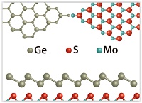
Germanene is a one atom thick sheet of germanium, in a honeycomb structure. It has clear similarities with graphene, the material that induced massive research activity worldwide, especially after 2010’s Nobel Prize. A major difference between graphene and germanene is the ‘band gap’, a property well-known in semiconductor electronics: thanks to this ‘jump’ of energy levels that electrons are allowed to have, it is possible to control, switch and amplify currents. Graphene had a very small band gap that can only be measured at very low temperatures, germanene shows a band gap that is significantly larger. Previous attempts to grow germanene, however, show that these attractive properties seem to vanish when it is grown on a metal surface: a good conductor of current. To prevent this, the UT scientists chose the semiconductor MoS2 as the substrate material.
Islands
Under ultra-high vacuum conditions, germanene indeed grows on the semiconductor. At first, the scientists observed islands at the locations where MoS2 had crystal defects, after that the germanene is spreading out covering a larger surface. An exciting question is, if the desired properties remain intact. First measurements show that the typical 2D properties and band gap are present, further low temperature measurements are needed to confirm that germanene operates in the desired way: the inner part would work as an insulator, while conducting channels are formed at the edges.
Sandwich
The other UT scientists did quantum mechanical calculations on the molybdenum-disulfide combination. They, for example, looked at the direction of growth, to be able to optimize the process. The theoretical group went one step further, by not only investigating the bilayer of molybdenum-disulfide, but als covering the germane with molybdeendisulfide. This prevents germanene from rapid oxidation. Calculations show that the sandwich construction has even better performance when it comes to the band gap.
Both publications show dat germanene, grown on molybdenum-disulfide is an important first step towards new electronic devices or unsuspected combinations with conventional devices. ‘Spintronics’, based on the spin movement of electrons, seems to be an attractive application area for germanene. Electrons with spin up and electrons with spin down have separate conducting channels on the edges of germanene. Harold Zandvliet recently received a grant for further research on this promising effect.
Share on:


Suggested Items
ZESTRON Academy Launches 2024 Advanced Packaging & Power Electronics Webinar Series
05/01/2024 | ZESTRONZESTRON, the leading global provider of high-precision cleaning products, services, and training solutions in the electronics manufacturing and semiconductor industries, proudly announces the launch of its highly anticipated webinar series on Advanced Packaging & Power Electronics, a webinar series on the latest innovations, cleaning, and corrosion challenges.
Worldwide Silicon Wafer Shipments Dip 5% in Q1 2024
05/01/2024 | SEMIWorldwide silicon wafer shipments decreased 5.4% quarter-over-quarter to 2,834 million square inches in the first quarter of 2024, a 13.2% drop from the 3,265 million square inches recorded during the same quarter last year, the SEMI Silicon Manufacturers Group (SMG) reported in its quarterly analysis of the silicon wafer industry.
Guerrilla RF Completes Strategic Acquisition of GaN Device Portfolio from Gallium Semiconductor
04/29/2024 | BUSINESS WIREGuerrilla RF, Inc. has finalized the acquisition of Gallium Semiconductor's entire portfolio of GaN power amplifiers and front-end modules. Effective April 26th, 2024, GUER acquired all previously released components as well as new cores under development at Gallium Semiconductor.
SIA Commends CHIPS Act Incentives for Micron’s Manufacturing Projects in New York and Idaho
04/29/2024 | SIAThe Semiconductor Industry Association (SIA) today released the following statement from SIA President and CEO John Neuffer applauding semiconductor manufacturing incentives announced by the U.S. Department of Commerce and Micron.
iNEMI Packaging Tech Topic Series: Role of EDA in Advanced Semiconductor Packaging
04/26/2024 | iNEMIAdvanced semiconductor packaging with heterogenous integration has made on-package integration of multiple chips a crucial part of finding alternatives to transistor scaling. Historically, EDA tools for front-end and back-end design have evolved separately; however, design complexity and the increased number of die-to-die or die-to-substrate interconnections has led to the need for EDA tools that can support integration of overall design planning, implementation, and system analysis in a single cockpit.