


 The Right Approach: I Hear the Train A Comin'
 It’s Only Common Sense: OCCAM—the Time Is Now
 Marcy's Musings: The Growing Industry
Scientists Explain Unusual and Effective Features in Perovskite
June 28, 2016 | Moscow Institute of Physics and TechnologyEstimated reading time: 2 minutes
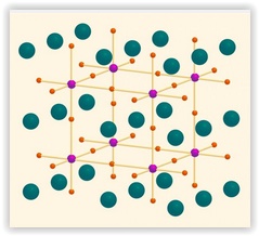
Perovskite is a material with an almost ideal structure. The majority of high-temperature superconductors are perovskite-based due to their non-ideal structure. The material can also be used to produce flexible solar batteries without rare-earth metals, which would help to reduce costs and enable large-scale manufacture.
One of the authors notes the manganite-like properties of perovskites. "This material exhibits many interesting and intriguing properties, most notably giant magnetoresistance. Many manganite properties are unknown, despite the fact that manganites have been studied for decades. We tried to work out what the conduction mechanism is of one of the most common compounds - Pr1-xCaxMnO3," he says. All these features have been experimentally discovered, but the processes to explain these unique properties are unknown.
Semiconductors were discovered more than 150 years ago. Electricity was a new development at the time. It was obvious that there were isolators like rubber and glass, conductors like copper and gold, and some uncertain materials, semiconductors, which did not fit into any category. The mechanisms of semiconductors remained unknown for about a century. It was not until the 1930s that the problem was solved and the first transistor was made. Nowadays it is difficult to imagine any electronic device without transistors.
Unfortunately, it is not possible to see charge movement in a material under a microscope. This is why researchers at Terahertz Spectroscopy Laboratory decided to use indirect detection methods. To test which particles are conductive, they applied different frequency voltages and measured the relationship between frequency and induced current. The scientists measured the frequency and temperature dependence of conductivity and permittivity in a broad frequency range (5-3000 cm-1) to cover all the bases. Wide temperature ranges - from 10 to 300 K (-263 to 27 °C) - of the samples were obtained to distinguish similar dependences of samples with different conduction mechanisms. But even this was insufficient to clarify the nature of charge carries. For this reason, researchers compared perovskites with different ratios of calcium (Ca) and praseodymium (Pr).
The group of scientists headed by Boris Gorshunov, Terahertz Spectroscopy Laboratory supervisor, (Lenar Kadyrov PhD, and laboratory scientists Elena Zhukova and Vladimir Anzin are also authors of this article) thus discovered that the charge carriers in Pr1-xCaxMnO3 perovskites are polarons. A polaron is an electron moving through the constituent atoms of a material, causing the neighboring positive charges to shift toward it and the neighboring negative charges to shift away. The properties of perovskites are ideal for electron-phonon (phonons are vibrations in a crystal lattice) coupling, determined by the interplay between symmetry breaking interactions. The researchers established that polarons move coherently (as one unit). That is to say charge carriers behave more like uncoupled particles. The idea of coherence is used in lasers, superconductors, highly accurate distance measurements, quantum calculations etc.
Establishing how conduction occurs could help perovskite research projects and large-scale applications to progress. For example, there is already a high-efficiency perovskite-based device for separating water into oxygen and hydrogen. Perovskites can also be used as LEDs, however they are currently only able to function at the temperature of liquid nitrogen.
Share on:


Suggested Items
Designer’s Notebook: What Designers Need to Know About Manufacturing, Part 2
04/24/2024 | Vern Solberg -- Column: Designer's NotebookThe printed circuit board (PCB) is the primary base element for providing the interconnect platform for mounting and electrically joining electronic components. When assessing PCB design complexity, first consider the component area and board area ratio. If the surface area for the component interface is restricted, it may justify adopting multilayer or multilayer sequential buildup (SBU) PCB fabrication to enable a more efficient sub-surface circuit interconnect.
Insulectro’s 'Storekeepers' Extend Their Welcome to Technology Village at IPC APEX EXPO
04/03/2024 | InsulectroInsulectro, the largest distributor of materials for use in the manufacture of PCBs and printed electronics, welcomes attendees to its TECHNOLOGY VILLAGE during this year’s IPC APEX EXPO at the Anaheim Convention Center, April 9-11, 2024.
ENNOVI Introduces a New Flexible Circuit Production Process for Low Voltage Connectivity in EV Battery Cell Contacting Systems
04/03/2024 | PRNewswireENNOVI, a mobility electrification solutions partner, introduces a more advanced and sustainable way of producing flexible circuits for low voltage signals in electric vehicle (EV) battery cell contacting systems.
Heavy Copper PCBs: Bridging the Gap Between Design and Fabrication, Part 1
04/01/2024 | Yash Sutariya, Saturn Electronics ServicesThey call me Sparky. This is due to my talent for getting shocked by a variety of voltages and because I cannot seem to keep my hands out of power control cabinets. While I do not have the time to throw the knife switch to the off position, that doesn’t stop me from sticking screwdrivers into the fuse boxes. In all honesty, I’m lucky to be alive. Fortunately, I also have a talent for building high-voltage heavy copper circuit boards. Since this is where I spend most of my time, I can guide you through some potential design for manufacturability (DFM) hazards you may encounter with heavy copper design.
Trouble in Your Tank: Supporting IC Substrates and Advanced Packaging, Part 5
03/19/2024 | Michael Carano -- Column: Trouble in Your TankDirect metallization systems based on conductive graphite or carbon dispersion are quickly gaining acceptance worldwide. Indeed, the environmental and productivity gains one can achieve with these processes are outstanding. In today’s highly competitive and litigious environment, direct metallization reduces costs associated with compliance, waste treatment, and legal issues related to chemical exposure. What makes these processes leaders in the direct metallization space?