


 Trouble in Your Tank: Understanding Interconnect Defects, Part 1
 It’s Only Common Sense: Marketing Isn’t Fluff, It’s Ammunition
 Driving Innovation: Mechanical and Optical Processes During Rigid-flex Production


The Newest Flex Shop in the U.S.
July 7, 2016 | Barry Matties and Angela Alexander, I-Connect007Estimated reading time: 27 minutes
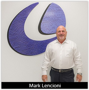
I-Connect007 sales team member Angela Alexander and I recently got a tour of Lenthor’s new Silicon Valley flex board shop and then sat down with President and CEO Mark Lencioni to discuss the new flex facility, the markets, management, and the future.
Barry Matties: Mark, give our readers a little background on Lenthor Engineering and what you do.
Mark Lencioni: We are entering our 31st year of business; having been founded in 1985. We are now located in our brand new, 55,000 sq. ft. state-of-the-art facility dedicated specifically to the fabrication and assembly of flex and rigid-flex products. We made it as “Lean” as possible for all our manufacturing systems to be very close to each other, in order to get the most efficiencies with our employees and product movement. It came out just like we planned.
Matties: So is Lenthor a flex shop primarily?
Lencioni: Yes, we specialize in flex circuit fabrication and assembly. We specialize in multilayer and rigid-flex technology, very high aspect ratios, high layer counts, and the technology to allow packaging to get into the size and shape it needs to be. We have succeeded by satisfying the toughest demands from the most demanding customers in the world.
Matties: Flex is still one of the fastest growing areas in the marketplace.
Lencioni: Yes, our customers’ products are the largest they will ever be and flex circuits are a natural solution to help people package things in the size and shape they need to be. They're getting smaller and smaller. From wearable devices, to cellphones, to any kind of mechanical device, automotive, military equipment, and some semiconductor equipment processing.
Matties: In your 30+ years, what's the most surprising thing you have seen in the flex market?
Lencioni: I would say the growth in both medical and military. We didn't really appreciate the opportunity these markets held for us until we did some specific market research after 9/11. The results of that research are what led us to move more heavily into these markets. If you look at the world and the environment we are in, these marketplaces are poised to be well-established for many, many years to come.
Matties: Your facility is an ITAR facility; what's the percentage of work that you bring through here?
Lencioni: We are about 55% military, 25% medical, and the rest balances across industrial and telecom.
Matties: Where do you see the largest growth coming from right now?
Lencioni: Military and Medical. Military obviously is in a very stable environment because it doesn't go offshore. We are finding growth from within a market that we are already well positioned to support. The medical market is also very favorable for us. We have developed the kind of process validation and control that market insists on.
Matties: Going back to your new facility, who laid out the facility?
Lencioni: It was a combination of Rich Clemente and myself. We took the processes, and with help from engineers regarding where they needed to be, we just started to lay it out. We did that with an architect, and so whatever building we decided to go into we just took that footprint and laid it right in.
Matties: When you are laying out a facility like this, what's the goal?
Lencioni: The goals were product efficiency and people movement. To really make sure that the product started finished within the most efficient process path, minimizing as best we could the movement and handling of materials.
Matties: When we first started the tour we talked about your old facility and the length of that process.
Lencioni: Yes, we had a campus environment previous to this which included three separate buildings. Although they were across the parking lot from each other, the movement of materials from beginning to end was about 2.2 miles. We re-validated what it is in our new factory and depending on product type the movement is down to about one eighth of a mile. The product moves with more efficiency, it doesn't get mishandled, and the employees are able to stay focused on their job of producing boards instead of moving materials.
Page 1 of 5
Share on:


Testimonial
"We’re proud to call I-Connect007 a trusted partner. Their innovative approach and industry insight made our podcast collaboration a success by connecting us with the right audience and delivering real results."
Julia McCaffrey - NCAB GroupSuggested Items
Trouble in Your Tank: Understanding Interconnect Defects, Part 1
11/04/2025 | Michael Carano -- Column: Trouble in Your TankThis month, I’ll address interconnect defects (ICDs). While this defect continues to rear its ugly head, don’t despair. There are solutions, most of which center on process control and understanding the relationship of the chemistry, materials, and equipment. First, though, let’s discuss ICDs.
WestDev Announces Advanced Thermal Analysis Integration for Pulsonix PCB Design Suite
10/29/2025 | WestDev Ltd.Pulsonix, the industry-leading PCB design software from WestDev Ltd., announced a major enhancement to its design ecosystem: a direct interface between Pulsonix and ADAM Research's TRM (Thermal Risk Management) analysis software.
Designers Notebook: Power and Ground Distribution Basics
10/29/2025 | Vern Solberg -- Column: Designer's NotebookThe principal objectives to be established during the planning stage are to define the interrelationship between all component elements and confirm that there is sufficient surface area for placement, the space needed to ensure efficient circuit interconnect, and to accommodate adequate power and ground distribution.
Episode 6 of Ultra HDI Podcast Series Explores Copper-filled Microvias in Advanced PCB Design and Fabrication
10/15/2025 | I-Connect007I-Connect007 has released Episode 6 of its acclaimed On the Line with... American Standard Circuits: Ultra High Density Interconnect (UHDI) podcast series. In this episode, “Copper Filling of Vias,” host Nolan Johnson once again welcomes John Johnson, Director of Quality and Advanced Technology at American Standard Circuits, for a deep dive into the pros and cons of copper plating microvias—from both the fabricator’s and designer’s perspectives.
Nolan’s Notes: Tariffs, Technologies, and Optimization
10/01/2025 | Nolan Johnson -- Column: Nolan's NotesLast month, SMT007 Magazine spotlighted India, and boy, did we pick a good time to do so. Tariff and trade news involving India was breaking like a storm surge. The U.S. tariffs shifted India from one of the most favorable trade agreements to the least favorable. Electronics continue to be exempt for the time being, but lest you think that we’re free and clear because we manufacture electronics, steel and aluminum are specifically called out at the 50% tariff levels.