


 Dan’s Biz Bookshelf: ‘The Next RenAIssance: AI and the Expansion of Human Potential’
 The Chemical Connection: When the Industry Moves Faster Than the Standards
 Driving Innovation: Selecting the Right Laser Source


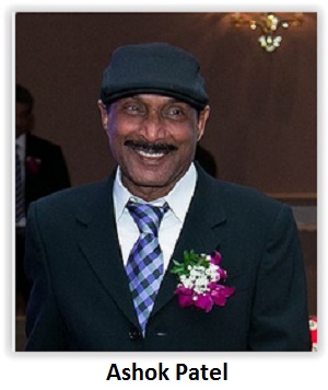
Catching up with Sunrise Electronics’ Ashok and Jigar Patel
July 12, 2016 | Dan BeaulieuEstimated reading time: 10 minutes
Located in the heart of Chicagoland’s PCB center in Elk Grove Village, Illinois, Sunrise Electronics builds some of the most sophisticated PCB products in the industry—and they build them fast. From 2-mil lines and spaces to sub 3-mil holes, to boards with special materials and metal-backed boards, this father and son, Ashok and Jigar, and their team can do it. In fact, there is little they cannot do. As Ashok told me, “When we have to ‘no bid’ a job I’ll keep the data and try to build the board until I get it right, and then I’ll call the customer back and tell him that we want to now bid. This has gotten us a lot of business since the customer has limited choices anyway, so he gives us a shot.”
I had been hearing about this company for many years, so when Ashok asked me to come and see them for myself, I jumped at the chance. It was one of the most amazing plant tours that I’ve been on in a long time. I wanted to know more, so we sat down and had a chat.
Dan: Ashok, please tell me a little bit about the history of the company.
Ashok: We founded the company in 1997 with the intention of doing exactly what we are doing now, which was to build boards quickly for people. I knew there was a great demand for prototype boards, especially high-tech boards. The company I was working with at the time wanted mostly production from larger companies and did not want to do business with smaller companies. I saw many benefits that someone could get if they were willing to work with those smaller companies, especially when they wanted technology that I knew not a lot of people could do. So we started this company and it has been successful from day one.
Dan: Tell me about what you can do in terms of the technology.
Ashok: We obviously can build your run-of-the-mill, 2−8 layer boards with 5-mil trace/space, but we are able to build product down to 1.5-mil trace/space as well and are continuously pushing the limits of design. A lot of times customers will come to us with a design that may have been shot down by another vendor due to certain design constraints; we view our relationship as a working partnership, and we work together to build a product that others may not be able to. We are willing to invest the time and money so that we can experiment and learn what is preventing us from being able to build it rather than decline the opportunity.
Jigar: We have really enhanced our capabilities on metal-core products as well. Aside from building the typical single-sided aluminum we also build 2-layer aluminum/copper core boards in many ways, one of which is to build it with the metal substrate in between the two copper layers and isolating vias from the metal to prevent shorting.
Dan: Can you give me some insight into your capabilities?
Jigar: Our specialty is and always will be quick-turn fabrication. Generally, our standard lead time is three days, so work is always flowing through the shop quickly and efficiently, allowing us to accommodate incoming quick-turn work regularly. We have later cutoff times than others in the industry. If someone comes to us at 11:00 a.m. and asks us to fab a 2-layer board and it needs to ship that evening, we will be able to do that. We typically have 2−3 orders like this on a daily basis, which are “same-day turn.” Can we do a 4−layer in a same day turn? Yes, but obviously that requires an early start and is contingent upon data.
Dan: You do rigid, flex and rigid-flex, metal-backed and special materials, right?
Ashok: Yes, we can build flex/rigid-flex.
Dan: I know you guys are doing a lot of cutting edge work. Tell me where you think technology is going today and in the future.
Ashok: Products these days are getting smaller and smaller, which is proven by the designs we are quoting and building. I see a greater need for more dense boards where 4/4 trace/space is the norm and 1/1or 2/2 is right around the corner. Nano technology comes to mind as well in the coming years.
Dan: Where do you rate Sunrise in terms of technology?
Jigar: I believe we sit at the top right next to the big guys. We have all the pieces in place, not only with regard to equipment, but also with our personnel.
Dan: Now let’s talk about quality. What are your qualifications and registrations?
Ashok: We have ISO and ITAR certs. We are not certified to Mil-Spec but can build to these certifications and on certain time-sensitive projects we have received waivers to build these products. We are a perfect fit for those who are looking at doing engineering and development builds. We work very closely with our customers and proof of concept and pushing the limits and capabilities of build in order to develop new processes and technologies. Since our lead-times are so short, it allows clients to develop proof of concept sooner and get product to market quicker.
Dan: What makes Sunrise stand out?
Jigar: The fact that we work very closely on product development and deliver 12−48 hour turns on a daily basis helps us help our clients execute more quickly than the rest. We value each of our clients and treat them as our partners. Nothing is more fulfilling than helping them grow their business, which is why a majority of our work comes from referrals. We truly believe in picking up the phone and calling, versus emails, as that adds the personal touch and service goes beyond just building a product. We always like to go that extra mile.
Dan: I know you work with a lot of new product development engineers. Can you talk about that and about the R&D work that you guys do?
Ashok: We have in the past had RFQs that we had to ‘no bid’ because our comfort level with the build was not quite there. However, instead of no bidding and forgetting about it we actually take the files and internally begin building the board to develop to the processes needed to build that type of product in the future. This is done at our own expense, but we learn from it and see value in the expenditure.
Dan: I love that. So you actually do this on your own dime?
Ashok: Yes, absolutely. Look, these people need these boards, they need this technology so we try to provide it to them if we can.
Dan: I know from our tour that you have invested in some new equipment lately. Can you tell us about that?
Jigar: We have made quite a few expenditures in the past year, adding the new Lenz driller/router, which allows us to drill and rout with 0.0005” accuracy. We purchased a via-fill and planarization machine, the Camtek gryphon soldermask/silk printer, and a brand new flying probe tester. We upgraded our AOI systems as well and in the near future we plan to add a pulse plating line. Our expenditures are not only limited to equipment; we have also spent money on personnel—it is very important to have the right people. You are only as good as the people you work with and there is great value in having the correct staff. We also expanded our facility by acquiring another 10,000 sq. ft. building to expand our drilling and lamination department. Between our main and second building, we operate under a total of 28,000 sq. ft.
Page 1 of 2
Share on:


Testimonial
"We’re proud to call I-Connect007 a trusted partner. Their innovative approach and industry insight made our podcast collaboration a success by connecting us with the right audience and delivering real results."
Julia McCaffrey - NCAB GroupSuggested Items
Driving Innovation: Selecting the Right Laser Source
04/28/2026 | Simon Khesin -- Column: Driving InnovationWhen I first joined Schmoll Maschinen, I brought experience from almost every PCB process, except for laser. As I immersed myself in laser processing, I realized why it can seem so daunting to a newcomer. The complexity arises from three intersecting factors: A vast variety of laser sources: CO2, UV-nano, green-pico, UV-pico, IR-pico, and others; a diverse range of applications: Drilling, cutting, ablation, and more; and an extensive list of materials: These have vastly different absorption rates. Choosing the right machine or laser source is rarely trivial. Even for experienced engineers, answering "Which source is best?" requires examining the business's specific goals.
Institute of Circuit Technology Spring Seminar 2026: A Bright Future in Europe
04/23/2026 | Pete Starkey, I-Connect007Through the leafy lanes and spring flowers of Warwickshire and back to Meridan, the traditional centre of England, and now officially part of the Metropolitan Borough of Solihull in the county of the West Midlands, I attended the Annual General Meeting and Spring Seminar of the Institute of Circuit Technology (ICT) on April 14. Out of the AGM came notable changes in leadership at the top of the Institute: the retirement of Mat Beadel as chair and Emma Hudson as technical director. Effective May 1, Steve Driver is the new chair, and Alun Morgan is the new technical director.
ACCM Unveils Negative and Near-zero CTE Materials for Large-Format AI Chips
04/21/2026 | Advanced Chip and Circuit MaterialsAdvanced Chip and Circuit Materials, Inc. (ACCM) has launched two new materials: Celeritas HM50, with a negative coefficient of thermal expansion (CTE) of -8 ppm/°C to offset the positive CTE and expansion of copper with temperature on circuit boards, and Celeritas HM001, with near-zero CTE and the low-loss performance needed for high-speed signal layers to 224 Gb/s and faster in artificial intelligence (AI) circuits.
Fresh PCB Concepts: Designing PCBs for Harsh Environments—Reliability Is Engineered Upstream
04/23/2026 | Team NCAB -- Column: Fresh PCB ConceptsWhen engineers hear the phrase “harsh environment,” they usually think of the extreme temperature swings, vibration and shock, pressure changes, or radiation in aerospace. However, aerospace is not the only harsh environment where electronic assemblies must survive. Automotive power electronics, downhole oil and gas tools, marine controls, rail systems, defense platforms, and industrial automation equipment all expose PCBs to environments that are equally unforgiving. The stress mechanisms may differ, but the physics does not.
Advanced Packaging for AI: Reliability Starts at the Cu/Cu/Cu Microvia Junction
04/20/2026 | Kuldip Johal, MKS' AtotechThe rapid growth of AI computing, from training clusters to inference at scale, is reshaping demand across the entire electronics supply chain. Advances in technology requirements, such as higher bandwidth, lower latency, and greater compute density, are driving the development of advanced packaging technologies and transforming the PCB industry across design, manufacturing, testing, and even architecture.