


 The Right Approach: I Hear the Train A Comin'
 It’s Only Common Sense: OCCAM—the Time Is Now
 Marcy's Musings: The Growing Industry
Controlling Anisotropy
July 25, 2016 | A*STAREstimated reading time: 2 minutes
The huge energy consumption of the world’s data centers creates an urgent need to develop electronic devices that can process information with reduced power requirements. A device that harnesses the ‘spin’ of electrons offers a route toward this. A*STAR researchers show how the performance of these so-called spintronic memories can be optimized by careful control of its structure.
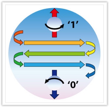
A spin-transfer torque magnetic random-access memory (STT-MRAM) comprises a stack of thin magnetic layers. One of these layers makes all the electrons in a current flowing through it have the same spin. This spin-polarized current can then change the magnetic properties of a second layer. This relies on the tendency of the electron spins in the material to align along one direction much more than it does another — a property called magnetic anisotropy.
“By having a high anisotropy, the magnet is stable and the memory is able to retain information,” explains Sze Ter Lim from the A*STAR Data Storage Institute. “However, it also means that it is more difficult to switch to the opposite direction because of an effect called damping.” Previous attempts to increase the anisotropy have also led to a proportional increase in damping.
Lim and his co-workers have now developed a STT-MRAM architecture in which the anisotropy can be increased without changing the damping. Their device has a central layer of tantalum. On either side of the central layer is a film of cobalt iron boron (CoFeB), which makes up the required magnetic layers. This in turn is sandwiched between magnesium oxide. The device is grown on a substrate and capped with another layer of tantalum.
Instead of altering the thickness of the magnetic layers, as previous studies have done, the researchers investigated the influence of the outer magnesium oxide. They showed that the anisotropy rises when the top layer thickness is increased from 1.3 nanometers to 2.5 nanometers. But the effect of this change on the damping is minimal.
Lim’s team however does not believe that this change in anisotropy is directly related to the thickness of the magnesium oxide; indeed, similar changes to the thickness of the bottom magnesium oxide film had no effect. Instead, they suggest that the top tantalum atoms intermixed with the magnesium oxide during deposition, and this degrades the interface between the magnesium oxide and the CoFeB.
“The next step is to integrate these optimized materials structures into practical devices and to evaluate its performance,” says Lim.
Share on:


Suggested Items
Designer’s Notebook: What Designers Need to Know About Manufacturing, Part 2
04/24/2024 | Vern Solberg -- Column: Designer's NotebookThe printed circuit board (PCB) is the primary base element for providing the interconnect platform for mounting and electrically joining electronic components. When assessing PCB design complexity, first consider the component area and board area ratio. If the surface area for the component interface is restricted, it may justify adopting multilayer or multilayer sequential buildup (SBU) PCB fabrication to enable a more efficient sub-surface circuit interconnect.
Happy’s Tech Talk #27: Integrated Mesh Power System (IMPS) for PCBs
04/08/2024 | Happy Holden -- Column: Happy’s Tech TalkA significant decrease in HDI substrate production cost can be achieved by reducing the number of substrate layers from conventional through-hole multilayers and microvia multilayers of eight, 10, 12, and more to only two layers. Besides reducing direct processing steps, the yield will increase as defect-producing operations are eliminated. The integrated mesh power system (IMPS) was invented in the latter years of MCM-D use for thin-film fabrication. Those geometries fit today into our use of ultra HDI.
Insulectro’s 'Storekeepers' Extend Their Welcome to Technology Village at IPC APEX EXPO
04/03/2024 | InsulectroInsulectro, the largest distributor of materials for use in the manufacture of PCBs and printed electronics, welcomes attendees to its TECHNOLOGY VILLAGE during this year’s IPC APEX EXPO at the Anaheim Convention Center, April 9-11, 2024.
Now Available: Episode 4, Season 2 of Designing for Reality—Lamination
04/04/2024 | I-Connect007I-Connect007 has just released the latest episode of its podcast series, On the Line With..., which focuses on designing for reality in the electronics industry. Multilayer boards bring along a completely different set of processes. In this installment, ASC Sunstone VP/Manager Matt Stevenson discusses manufacturing techniques for multilayer boards. Of course, this necessitates a review of drill and registration techniques, followed by the ins and outs of lamination.
Heavy Copper PCBs: Bridging the Gap Between Design and Fabrication, Part 1
04/01/2024 | Yash Sutariya, Saturn Electronics ServicesThey call me Sparky. This is due to my talent for getting shocked by a variety of voltages and because I cannot seem to keep my hands out of power control cabinets. While I do not have the time to throw the knife switch to the off position, that doesn’t stop me from sticking screwdrivers into the fuse boxes. In all honesty, I’m lucky to be alive. Fortunately, I also have a talent for building high-voltage heavy copper circuit boards. Since this is where I spend most of my time, I can guide you through some potential design for manufacturability (DFM) hazards you may encounter with heavy copper design.