


 SMT Prospects and Perspectives: AI Opportunities, Challenges, and Possibilities, Part 1
 Nolan’s Notes: Do More, Get More
 Global Sourcing Spotlight: Don’t Be Afraid of Global Sourcing
Nondestructive Inspection of Underfill Layers Stacked up in Ceramics-Organics-Ceramics Packages with SAT
August 16, 2016 | F. Sarrazin, et al.*Estimated reading time: 4 minutes
Ceramics packages are being used in the electronics industry to operate the devices in harsh environments. In this paper, we report a study on acoustic imaging technology for nondestructively inspecting underfill layers connecting organic interposers sandwiched between two ceramics substrates. First, we inspected the samples with transmission mode of scanning acoustic tomography (SAT) system, an inspection routine usually employed in assembly lines because of its simpler interpretation criteria: flawed region blocks the acoustic wave and appears darker. In this multilayer sample, this approach does not offer the crucial information at which layer of underfill has flaws. To resolve this issue, we use C-Mode Scanning in reflection mode to image layer by layer utilizing ultrasound frequencies from 15MHz to 120MHz. Although the sample is thick and contains at least five internal material interfaces, we are able to identify defective underfill layer interfaces.
Introduction
Since introduction of scanning acoustic tomography (SAT) also known as C-Mode scanning acoustic microscopy (CSAM) technology to the semiconductor package manufacturing for more than two decades, several thousand pieces of equipment have been serving the industry as essential quality assurance tools. Acoustic imaging offers inspection of imperfect material joints containing non-metal structures, such as delamination between silicon-metal joint glues, which in turn are difficult if not impossible to detect with X-ray imaging approach. Therefore, the device package failure analysis engineers routinely utilize both x-ray and acoustic imaging technologies as their complimentary nondestructive analysis tools.
The SAT technology does have its own limitations derived from the physical nature of acoustical wave: requirement of liquid medium to transfer ultrasound energy, requirement of flat and smooth package surface, difficulty in designing transducers, low resolution at lower ultrasound frequencies, less penetration at higher ultrasound frequencies, and slow acquisition speeds, etc.
To extend these limitations to their ends, development of new transducers or probes with applicable frequency range from 50MHz to 300MHz are very crucial, along with other signal handling advancements.
Recently, Kitami, et al., reported development of a specially designed signal processing unit and high resolution probes that can image 1µm features engraved in silicon material and an echo gating technique that intelligently tracks the surface plane so that it drastically reduces invisible area due to rough exterior surfaces of the package.
Encouraged by these new developments, we conducted a case study of SAT and X-ray CT imaging for a multilayer package consisting of two ceramics with flip-chip packages on organics substrates in between. The SAT system available for this study is also equipped with high resolution unit that generates well compressed pulses with excellent signal to noise ratio in a wide range of probe frequencies. In this report, we describe how flaws around flip-chip substrates embedded in a thick stack of ceramics mounted with surface components can be nondestructively inspected layer by layer to pinpoint the manufacturing defects hidden in them.
Experimental
On the manufacturing floor, we noticed that some of the multilayer devices electrically failed but they were also unable to find out the root cause using existing analytical equipment. Cross sectioning the sample is the only option which is not only destructive but also time consuming just to find out about the flaws along one line out of entire surface. Therefore, we selected to study the most acoustically complex device to investigate the capability with state of the art X-ray and ultrasound imaging technologies.
Sample Descriptions and Preview
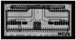
The sample consists of high temperature co-fired ceramics (HTCC) substrates as top and bottom layers embedded with chip packages on polymer substrates in between as illustrated in Figure 1. The dimensions are 18 mm width, 35 mm length, and 3.3 mm height. The regions of interest for possible delamination or voids are the joints to each interfaces between deep layers. Of course, these HTCC layers themselves are multi-layered substrates as well.
Figure 1: Illustration of material structure of the sample and their thickness in micrometer. Outer layers are high-temperature, co-fired ceramics.
So far we have accumulated some knowledge on computed tomography (CT) inspection of various complex structures, especially for solder joints with good and clear CT images. This ceramics package, however, was just quickly viewed with an X-ray CT system to find out any flaws in metal features and ceramics layers. 3D-CT inspection revealed that there are no apparent flaws in the material layers themselves; but no further attempts were made with CT inspection because it is difficult to observe delamination type of flaws between materials given the nature of X-ray beam that can easily penetrate such a flaw without significant intensity reduction. Comprehensive study with X-ray CT maybe needed elsewhere.
SAT Imaging
During manufacturing process at the beginning, the samples were inspected with available CSAM system without much success, pointing at that complicated sample structure; eventually requiring destructive cross sectioning. For nondestructive inspection, it is challenging to construct acoustic image of multilayer structures, because the echoes usually involve multiple reflections as well as their interferences. The difficulty increases when the sample is thicker as it requires lower frequency acoustic beam with smallest possible beam spot at longer focal lengths to reach deep layers. To overcome these hurdles, we need to get optimized transducers suitable to this particular sample.
All SAT results presented in this paper are from a new SAT system with high resolution unit option. This new SAT system has better capabilities covering transducer frequencies from 5MHz to 300MHz at prescribed frequencies, and especially with high resolution hardware option the user can virtually set any desired ultrasound frequencies that should fit to a particular sample conditions.
To read this entire article, which appeared in the August 2016 issue of SMT Magazine, click here.
Share on:


Suggested Items
Warm Windows and Streamlined Skin Patches – IDTechEx Explores Flexible and Printed Electronics
04/26/2024 | IDTechExFlexible and printed electronics can be integrated into cars and homes to create modern aesthetics that are beneficial and easy to use. From luminous car controls to food labels that communicate the quality of food, the uses of this technology are endless and can upgrade many areas of everyday life.
Trackwise Awarded Prestigious King’s Award for Enterprise for Innovation
04/24/2024 | TrackwiseTrackwise Designs plc, the innovative manufacturer of specialist products using printed circuit technology, is delighted to be recognised with a prestigious King’s Award for Enterprise. Announced, Friday 21 April, Trackwise has been recognised for its excellence in Innovation for its length-unlimited, multilayer flexible printed circuits.
Real Time with... IPC APEX EXPO 2024: Integrating Automation into the North American PCB Market
04/18/2024 | Real Time with...IPC APEX EXPODan Beaulieu introduces James Chien from SAA Symtek Automation Asia and Jason Perry from Technica, who are bringing automation to the North American PCB market. They discuss their expertise in automation, equipment sets, and growing opportunities. The focus is on integrating automation into existing shops, considering hardware, software, and flexibility. They also discuss the challenges of modernizing domestic shops and the potential of expanding automation to other markets.
Three Industry Leaders Receive IPC President’s Award
04/17/2024 | IPCIn recognition of their leadership and significant contributions of time and talent to IPC and the electronics industry, three IPC volunteers were presented with the IPC President’s Award at IPC APEX EXPO in Anaheim, Calif., on April 9, 2024.
IDTechEx Discusses the Role of Printed Sensors in Mass-Digitization
04/11/2024 | PRNewswireIntegrated sensors digitizing physical interactions are vital in everyday life. From personalized user experiences to warehouse inventory management, data-driven insights are driving demand for smarter sensors — and lots of them.