


 Dan’s Biz Bookshelf: Four Important Books You Need to Read (Not Just Say You Have)
 The Marketing Minute: Cracking the Code of Technical Marketing


Driven to Diffraction
November 15, 2016 | King Abdullah University of Science and TechnologyEstimated reading time: 3 minutes
As anyone with an interest in photography will know, to get features such as a powerful zoom, you usually need a big camera. The reason is that most cameras rely on refraction, whereby the light passing through lenses slows down and changes direction. Focusing this refracted light requires a certain amount of space.
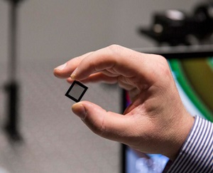
A promising route to smaller, powerful cameras built into smartphones and other devices is to design optical elements that manipulate light by diffraction-the bending of light around obstacles or through small gaps-instead of refraction.
Wolfgang Heidrich and co-workers at KAUST's Visual Computing Center and the University of British Columbia (UBC) in Canada are at the forefront of developing new diffractive optical elements (DOEs) that can be printed on to small, thin substrates. The team combines their carefully-designed DOEs with advanced computational techniques that can greatly enhance the images produced by such small optical devices.
Heidrich came to KAUST in 2014 from UBC, where he previously developed very high contrast displays for television sets.
"We developed the first consumer-ready display technology that had a major computational component, in the sense that the hardware itself was not useful without substantial computation," he says. "The target image would be sent to the device, and then the device would have to perform some fairly sophisticated algorithms on the image (in real time!) to produce the best image contrast. It really instilled in me the need for hardware-software co-design, where you develop optics, electronics and algorithms at the same time so that they fit together in the best possible way."
More recently, Heidrich and co-workers have applied the same approach to computational imaging for cameras. One major problem they are addressing, called chromatic aberration, will be familiar to anyone who has played with triangular prisms to produce a rainbow - different wavelengths change direction by varying amounts when they are refracted by lenses, resulting in incorrect color distributions in images.
Chromatic aberration is an even greater problem when light is manipulated by diffraction, so DOEs suffer a loss of color fidelity and blurring that depends on the color distribution of the incoming light. To combat this, Heidrich and his co-workers designed a thin, light-weight DOE called a diffractive achromat to balance the focusing contributions of different wavelengths. Their results from testing this innovative new component were published in ACM Transactions on Graphics ("The diffractive acromat: full spectrum computational imaging with diffractive optics") , the top journal destination for computer graphics studies.
"In a regular DOE lens, the focus will be near-perfect for a single design wavelength, and progressively blurred as you move away from that design wavelength," explains Heidrich. "The diffractive achromat sacrifices a little bit of sharpness for the design wavelength in exchange for more sharpness at all other wavelengths. Any remaining blur can then be removed computationally."
The researchers applied the same combination of cutting-edge optics with computer algorithms in a recent study published in Scientific Reports ("Encoded diffractive optics for full spectrum computational imaging") that could lead to extremely small zoom lenses. They used computational algorithms to design two DOEs with particular shapes, such that when they are placed on top of each other, they represent a diffractive lens with a specific focal length.
Then comes the cleverest bit.
"As you rotate the two DOEs relative to each other, the focal length, or any other parameter of the optical system, can change smoothly," says Heidrich. "One obvious application is to produce zoom lenses that do not require the lens barrel to move in and out of the camera for zooming."
Heidrich believes the active research environment at KAUST has been invaluable for pursuing his recent goals. "I have been able to assemble an interdisciplinary team, for more ambitious projects that take our hardware-software co-design to the next level," he says. "What's more, all our diffractive optical elements were built in the KAUST Nanofabrication Core Lab, which allowed quick turn-around times for experiments."
Computational imaging is still in its infancy, and provides many avenues that Heidrich and his co-workers hope to explore in coming years. Perhaps most excitingly, because DOEs are so thin, they don't absorb much energy from light as it passes through. This means that DOEs could, in principle, be used to manipulate any part of the electromagnetic spectrum, from radio waves to gamma rays.
Share on:


Testimonial
"In a year when every marketing dollar mattered, I chose to keep I-Connect007 in our 2025 plan. Their commitment to high-quality, insightful content aligns with Koh Young’s values and helps readers navigate a changing industry. "
Brent Fischthal - Koh YoungSuggested Items
Accelerating Embedded Innovation: Orthogone Becomes Texas Instruments Design Partner
09/17/2025 | PRNewswireOrthogone Technologies Inc., a leader in advanced embedded systems and FPGA development, is proud to announce its official designation as a Texas Instruments (TI) Design Services Partner.
BLT Joins Microchip Partner Program as Design Partner
09/17/2025 | BUSINESS WIREBLT, a U.S.-owned and operated engineering design services firm announced it has joined the Microchip Design Partner Program.
Staying on Top of Signal Integrity Challenges
09/16/2025 | Andy Shaughnessy, Design007 MagazineOver the years, Kris Moyer has taught a variety of advanced PCB design classes, both online IPC courses and in-person classes at California State University-Sacramento, where he earned his degrees in electrical engineering. Much of his advanced curriculum focuses on signal integrity, so we asked Kris to discuss the trends he’s seeing in signal integrity today, the SI challenges facing PCB designers, and his go-to techniques for controlling or completely eliminating SI problems.
American Standard Circuits to Exhibit and Host Lunch & Learn at PCB West 2025
09/17/2025 | American Standard CircuitsAnaya Vardya, President, and CEO of American Standard Circuits/ASC Sunstone Circuits has announced that his company will once again be exhibiting at PCB West 2025 to be held at the Santa Clara Convention Center on Wednesday, October 1, 2025.
ASM Technologies Limited signs MoU with the Guidance, Government of Tamilnadu to Expand Design-Led Manufacturing capabilities for ESDM
09/15/2025 | ASM TechnologiesASM Technologies Limited, a pioneer in Design- Led Manufacturing in the semiconductor and automotive industries, announced signing of Memorandum of Understanding (MoU) with the Guidance, Government of Tamilnadu whereby it will invest Rs. 250 crores in the state to expand its ESDM related Design-Led Manufacturing and precision engineering capacity. ASM Technologies will acquire 5 acres of land from the Government of Tamilnadu to set up a state-of-the-art design facility in Tamil Nadu's growing technology manufacturing ecosystem, providing a strong strategic advantage and long-term benefits for ASM.