


 It’s Only Common Sense: Customers Capabilities—and Confidence
 Dan’s Biz Bookshelf: ‘The 'NVIDIA Way: Jensen Huang and the Making of a Tech Giant’


Showing Some Constraint: Design007 Magazine July 2025
July 10, 2025 | I-Connect007 Editorial TeamEstimated reading time: Less than a minute
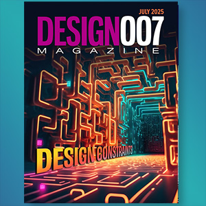
Constraints shape the entire PCB industry, and every design decision introduces trade-offs, often leading to more trade-offs. Nearly every element on the board can become a constraint depending on the end product: component and drill sizes, trace widths and spacing, material choices, microvias, testing requirements, signal and power integrity, thermal demands, fabricator limitations, and supply chain risks. The list doesn't stop there. It can also include compliance with FCC, FDA, UL, and ITAR regulations.
Building a smart constraint strategy that balances electrical and manufacturing needs takes deep experience, often years in the making. Fortunately, our expert contributors, many of whom are also educators, bring exactly that level of insight. This month, we explore design constraints: the essential requirements, common challenges, and proven best practices for getting them right.
Share on:


Testimonial
"In a year when every marketing dollar mattered, I chose to keep I-Connect007 in our 2025 plan. Their commitment to high-quality, insightful content aligns with Koh Young’s values and helps readers navigate a changing industry. "
Brent Fischthal - Koh YoungSuggested Items
Making AI Practical for PCB Design
03/05/2026 | Steve Watt, ZukenArtificial intelligence has entered nearly every corner of engineering software. In PCB design, however, meaningful adoption has been slower and for good reason. Unlike image generation or text analysis, PCB layout is not a data-rich, rules-light problem. It is a precision-driven engineering discipline in which creativity, accuracy, and strict compliance with constraints must coexist. Zuken’s work on AI-assisted PCB design reflects this reality. Rather than positioning AI as a replacement for engineering expertise, our CR-8000 Autonomous Intelligent Place and Route (AIPR) applies machine learning selectively in ways that align with how designers actually think and work.
Beyond Design: Managing Linear Workflow Bottlenecks
01/08/2026 | Barry Olney -- Column: Beyond DesignThe PCB design flow is sequential by nature, transitioning through distinct yet interdependent phases, from initial back-of-the-envelope concept sketches to schematic capture, constraint definition, physical layout, verification, and finally, generation of CAM deliverables. Each stage builds upon the last, and any delay, however minor, can cascade downstream, amplifying pressure on subsequent phases.
Target Condition: Floor Planning Without a Floor
08/27/2025 | Kelly Dack -- Column: Target ConditionBy a show of hands, how many PCB designers have been asked to start a layout without a board outline, keep-out zones, or even height constraints? How many have had to work within a specific enclosure before the schematic was finalized? If this sounds familiar, you're not alone. Starting a PCB layout without critical constraints is like hiring an interior designer to buy furniture and carpet for a house you haven’t even purchased yet, or, even worse, trying to fit four bedrooms' worth of furniture in a one-room cabin.
Getting Our ‘Fil’ of Design Constraint Techniques
08/07/2025 | Andy Shaughnessy, Design007 MagazineFilbert Arzola is a principal electrical engineer at Raytheon SAS and an instructor who teaches one of the few classes (that I know of) that focuses on setting design constraints. I asked Fil to share his thoughts on design constraints: the factors involved, the various trade-offs, and his best practices for optimizing constraints for your particular design. As Fil says, “Everything about a PCB is a constraint.”
Setting Design Constraints Effectively
07/31/2025 | Stephen V. Chavez, Siemens EDAPCB design requires controlling energy within the medium of a PCB. The manner in which we control the chaos of energy is by implementing and utilizing physical and electrical rules, known as constraints, along with a specific structure and material(s) that make up what is known as the foundation of the design. These rules govern everything within the PCB structure and generally fall into two camps: performance and manufacturability. Setting this foundation correctly is extremely important and the key to success.